Sensory & Nuclear Safety
Enterprise-grade Turnkey PCBA, High-Density Interconnects (HDI), and Multi-Layer System Integration. Precision engineering from Shenzhen’s certified smart production ecosystem to accelerate global hardware scale.
Verified Surface Mount Technology (SMT) and Through-Hole (THT) production for industrial automation, automotive drive units, and precision metrology.
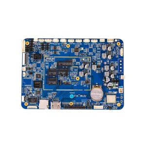

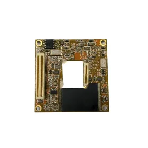
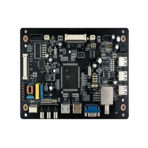

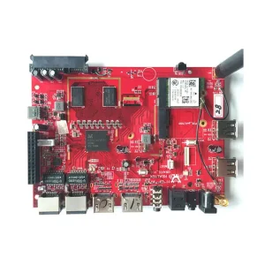
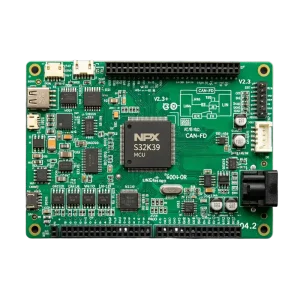
Analyzing procurement dynamics, supply chain decentralization, and high-complexity demands driving global tech original equipment manufacturers (OEMs).
Global procurement directors face rising challenges in raw material volatility, component obsolescence, and geopolitical disruption. Modern EMS providers must offer dual-track BOM sourcing, active lifecycle forecasting, and dynamic alternative approvals without altering core PCB schematics.
With edge AI devices, high-speed telecommunications, and sub-system automotive ECUs saturating the market, standard FR-4 processing is no longer sufficient. Production requires microvia drilling, blind/buried via architectures, and tight impedance tolerances across high-frequency RF substrates.
Western and global hardware innovators mandate end-to-end data custody. Engineering file transfers, firmware flashing, and functional verification require secure physical networks, automated lot tracking via Manufacturing Execution Systems (MES), and strict Non-Disclosure Protocols.
Eliminate multi-vendor friction. Our fully managed engineering chain integrates board design review, precision fabrication, component logistics, and system-level validation.
Before copper touches dry film, our 50+ staff engineers execute automated and manual Design for Manufacturability (DFM) and Design for Assembly (DFA) audits to avoid thermal shadowing, solder bridging, and component collision risks.
Harnessing a direct network of 100+ authorized global component suppliers and over 500,000 verified SKUs. We guarantee genuine Silicon, provide anti-counterfeiting test reports, and resolve lead-time bottlenecks.
Operating 7 high-speed SMT lines capable of 01005 passives and ultra-fine pitch 0.3mm BGA packages. Dual reflow setups feature multi-zone inert nitrogen control to ensure pristine joint morphology on complex assemblies.
From automated conformal coating and IC flashing to final enclosure assembly and full functional environmental stress screening (FCT/ESS), delivering turn-key hardware boxed and directly deployable to target markets.
Quantitative technical benchmarks adhered to across prototyping, pilot series, and mass-scale production runs.
| Process Parameter | Standard PCB Capability | Advanced HDI & RF Processing | Quality Verification Baseline |
|---|---|---|---|
| Layer Count & Stack-up | 1 - 8 Layers (Standard FR-4) | Up to 32 Layers (Rigid, Flex, Rigid-Flex, HDI) | IPC-6012 Class 2 / Class 3 |
| Min. Line Width / Space | 4 mil / 4 mil (0.10mm) | 2 mil / 2 mil (0.05mm) via LDI Lithography | AOI Microscopic Geometry Verification |
| Via Technology | Standard Through-hole (0.2mm) | Laser Microvia (0.075mm), VIPPO, Staggered/Stacked | Cross-sectioning & Metallographic Polish |
| Surface Finishes | HASL, Lead-free HASL, OSP | ENIG, ENEPIG, Immersion Silver/Tin, Hard Gold Plating | X-Ray Fluorescence (XRF) Thickness Gauge |
| SMT Placement Resolution | 0201 Components, 0.5mm Pitch | 01005 Components, 0.3mm BGA, PoP (Package on Package) | 3D SPI & 3D AOI Closed-Loop Feedback |
| Joint Integrity Verification | Visual & Standard 2D AOI | Offline 3D X-Ray Computed Tomography (CT), ICT & FCT | IPC-A-610 Class 3 Workmanship Standard |
How our engineering infrastructure evolves to meet the computing densities and environmental mandates of emerging computing architectures.
Full integration of hybrid laminate production (Rogers dielectric with standard high-Tg FR-4 cores) and commercial volume assembly for 77GHz radar and optical transceivers.
Integration of active passives and thin-core silicon dies embedded directly within inner substrate layers, slashing parasitic inductance and reducing board surface footprint by 40%.
Fabrication techniques incorporating optical waveguides inside the multilayer PCB stack to eliminate copper loss in high-throughput AI accelerator cards and server backplanes.
Deep neural network predictive modeling adjusting reflow profiles and squeegee pressure real-time, coupled with closed-loop wastewater and micro-etch copper circular recovery.
Providing Western enterprise clients frictionless collaboration through native technical communication, regulatory adherence, and strict legal compliance.
Certified automotive quality control system enforcing APQP, FMEA, PPAP level 3 submissions, and strict defect prevention mechanisms.
Stringent medical device standard ensuring comprehensive risk assessment, clean-room assembly, and component batch-level traceability.
Internationally audited operational quality, safety parameters, environmental stewardship, and green manufacturing protocols.
Full adherence to global chemical toxicity restrictions and UL 94V-0 flammability ratings backed by verified laboratory certificates.
Addressing engineering evaluations, logistics, intellectual property protection, and production scaling workflows.
Our DFM/BOM engineering analysis compares your bill of materials against real-time global distributor inventories. If a critical microchip or passive component is unavailable, our team identifies functional form-fit-function (FFF) alternatives, submits datasheets and electrical impact studies, and only proceeds upon formal client sign-off.
Yes. We operate with strict No MOQ constraints for initial engineering validation, NPI runs, and design verification tests (DVT). Once validated, the exact same machine programs, reflow profiles, stencil specifications, and test fixtures are migrated directly onto our mass production lines without re-qualification friction.
We execute standard mutual NDAs before any Gerber, schematic, or BOM exchange occurs. During programming, encrypted IC flashing setups ensure hex codes and proprietary algorithms cannot be read back or exported. Factory production floors operate under strict restricted access with isolated internal servers.
To provide a full turn-key PCB and assembly quote within 24 hours, we require: (1) RS-274X or ODB++ Gerber files, (2) Detailed Bill of Materials (BOM) detailing manufacturer part numbers and approved alternates, (3) Centroid / Pick-and-Place file, and (4) Clear assembly notes or functional testing specifications.
All micro-BGA and leadless packages (QFN, DFN) undergo automated 3D X-Ray Inspection (AXI) to assess ball shape, alignment, and void percentages. Our nitrogen-assisted reflow parameters maintain void rates significantly below the IPC-A-610 Class 3 upper threshold limit of 25% (typically maintaining <10%).
For urgent engineering prototypes, bare board fabrication can be delivered within 24–48 hours, while complete turnkey PCBA prototypes (with in-stock silicon) can ship in as fast as 3–5 working days via express international air freight (DHL, FedEx, UPS) directly to your lab or distribution hub.
Explore certified PCBA solutions engineered for mission safety, high-bandwidth networks, avionics telemetry, and distributed power systems.