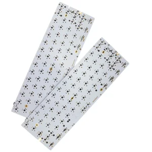
High-performance LED Printed Circuit Board Assemblies engineered for critical thermal dissipation, lumen stability, and extended operational longevity across architectural, commercial, and industrial deployments.
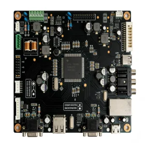
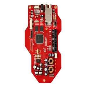
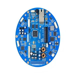
Analyzing the technological inflection point across solid-state lighting, automotive smart photonics, and human-centric commercial illumination architectures.
Modern LED dies convert only 30-40% of input electrical energy into photons; the remaining 60-70% degrades into parasitic junction heat. High-lumen solid-state systems require thermal management strategies moving beyond basic FR-4 toward Metal Core PCBs (MCPCB), direct-plated copper (DPC) ceramic substrates, and thermoelectric integration with thermal conductivity exceeding 3.0 W/m·K to eliminate thermal runaways.
Industrial vision and digital signage demand ultra-fine pitch matrix arrays (pitch < 0.9mm). This migration presents extreme assembly hurdles, requiring advanced solder paste jetting, vacuum reflow soldering to maintain void rates below 5%, and automated optical-inspection (AOI) setups capable of resolving microscopic bridging without sacrificing mass manufacturing speed.
Global OEM/ODM developers face supply friction across high-performance laminates, copper foils, and specific bin-sorted phosphor diodes. Certified manufacturing hubs with 100+ vetted tier-one semiconductor channel agreements eliminate binning mismatches, guarantee chromatic consistency (MacAdam Ellipse within 3 steps), and ensure continuous production resilience.
Overcoming manufacturing bottlenecks through tailored stack-up engineering, precision mechanical interfacing, and automated multi-zone surface-mount technology.
Tailored for floodlighting, high-bay fittings, and automotive forward headlights. We build Single-Layer, COB (Chip-on-Board), and Direct Thermal Path (DTP) boards using aluminum alloys (6061/5052) and electrolytic copper backing with dialectric breakdown voltage exceeding 4kV AC.
Enabling complex curved architectural contours and lightweight aerospace cabin lighting. Utilizing roll-to-roll (R2R) continuous automated SMT lines up to 50 meters, with ultra-thin polyimide bases and immersion silver/gold plating to prevent crack formation under cyclic bending.
SMT integration of onboard constant-current drivers, microcontrollers (MCU), DALI-2, ZigBee, and BLE mesh communication interfaces. Surface layout designed to isolate RF noise from high-frequency switching circuits, ensuring electromagnetic compatibility (EMC).
Bridging Shenzhen's world-class high-speed production lines with international quality frameworks to mitigate technical risk and guarantee field reliability.
Strict APQP and PPAP documentation, continuous thermal cycling stress runs (-40°C to +125°C), and automated solder paste inspection (SPI) for ADAS and matrix headlight assemblies.
Cleanroom production environments with documented batch tracking, specialized conformal coating against bio-contaminants, and surgical shadowless lamp array manufacturing.
All soldering, component placement, and board fabrication strictly conform to IPC-A-610 standards, verified via 3D Automated Optical Inspection (AOI) and High-Resolution X-Ray.
100% RoHS, REACH, CE, and UL certified material bases. Complete traceability from incoming resin and raw copper rolls to finished ESD hermetically packed crates.
Real-world implementation engineering designed to handle harsh outdoor elements, severe vibration, and extreme photobiological demands.
Assemblies incorporating multi-wavelength LED chips (deep red 660nm, far-red 730nm, UV 385nm, and high-CRI white). Formulated with high-transmittance silicone conformal coats to resist 95% relative humidity and volatile greenhouse agrochemicals.
Massive luminous flux demands (up to 150,000 lumens) requiring multi-kW power drive handling. We employ Direct-Bond-Copper (DBC) ceramic boards and heavy-copper PCBs (3oz-6oz) to conduct extreme thermal energy away from tight emitter matrices.
Deployments in transportation terminals, avionics displays, and outdoor UHD videowalls. Emphasizing low electromagnetic radiation, anti-sulfuration chip resistor integration, and high black-mask contrast solder masks for outdoor visibility.
Exhaustive parameters detailing manufacturing thresholds, machinery specifications, and metallurgical validation rules.
| Base Materials Handled | FR-4 (Tg 140°C - 180°C), Aluminum Core (1.0W to 8.0W/m·K), Copper Core, Ceramic (Al2O3 / AlN), Polyimide (Flex) |
|---|---|
| Max Board Dimensions | Standard SMT: 510mm x 460mm; Continuous Linear SMT Lines: Up to 1500mm single board / 50m roll-to-roll flex |
| Component Package Range | 01005 (0402 metric), 0201, CSP, Flip-Chip, QFN, BGA (0.35mm pitch), High-Power LEDs (3030, 3535, 5050, 7070, COB) |
| Dielectric Layer Thickness | 50μm, 75μm, 100μm, 125μm with high withstand breakdown voltage (>3000V - 6000V AC) |
| Thermal Conductivity | MCPCB: 1.0 - 8.0 W/m·K; Direct Thermal Path (DTP Copper): ~400 W/m·K; Ceramic: 24 - 180 W/m·K |
| Solder Types & Fluxes | Lead-Free SAC305, SAC0307, Low-temperature Sn-Bi alloys (for temperature-sensitive optical silicone lenses) |
| Verification & Quality Control | Inline 3D SPI, High-Speed Dual-Lane 3D AOI, 3D X-Ray Computed Tomography, High-Voltage Hi-Pot Testing, Thermal Imaging |
| Traceability Protocols | MES-driven real-time logging, 2D Data Matrix code laser etching on each PCB individual unit |
From digital Gerber verification through advanced automated SMT placement to final electro-optical burning.
Gerber and BOM engineering validation assessing pad footprint geometry, thermal via relief, and heat plane balance before tooling.
Direct factory sourcing across Cree, Lumileds, Osram, and Seoul Semiconductor ensuring identical luminous flux, CCT, and voltage bins.
Electro-polished nano-coated stencils with automated 3D SPI checks ensuring consistent paste volume under miniature optical pads.
Ultra-accurate pick-and-place lines running up to 80,000 CPH with dedicated optical nozzles that prevent mechanical scratching on silicon lenses.
10-zone nitrogen-purged reflow chambers keeping peak delta-T below 2°C across massive aluminum heat dissipation slabs.
Automated inspection determining void ratios (<10%), cold joints, solder bridges, and component misalignments with 100% digital records.
100% active operational burn-in cycles, color temperature spectrometer audits, vacuum anti-static shielding, and expedited global fulfillment.
Backed by complete IATF 16949, ISO 9001, and ISO 13485 accreditations, delivering a 99% shipment approval rate.
Strategic directions driving modern research and manufacturing investments over the upcoming decade.
Advancing past traditional vacuum mechanical nozzles toward high-speed elastomer stamp transfer and laser-assisted bonding (LAB). Targeting placement speeds exceeding 25,000 dice per hour with pitch boundaries shrinking below 50 microns for next-gen cockpit heads-up displays.
Embedding active driver ICs directly within internal PCB core substrate cavities. This strategy compresses overall module thickness by 65%, eliminates external wire-bonding choke points, and minimizes parasitic impedance for ultra-fast PWM dimming refresh rates.
Pioneering eco-friendly transient electronics. Exploring natural fiber composite laminates, water-soluble solder fluxes, and low-energy laser soldering processes that drastically slash lifecycle greenhouse carbon footprints in compliance with EU Circular Economy mandates.
Clear, direct answers regarding design optimization, volume delivery, material selection, and quality systems.
Engineered for intense lumen outputs, extreme thermal gradients, horticultural spectrum control, and rugged industrial signage environments.