Engineered to rigorous signal integrity, thermal dissipation, and functional verification benchmarks across high-consequence operational environments.
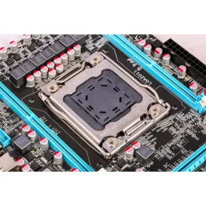
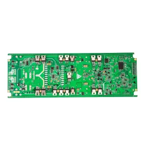
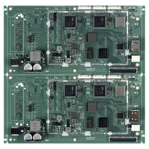
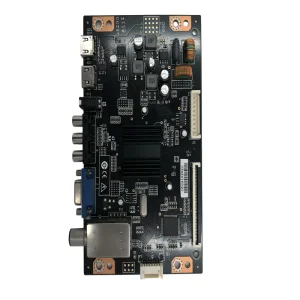
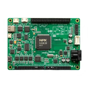
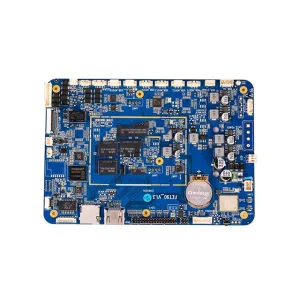

As processing silicon migrates to sub-3nm nodes and bus transfer rates cross 32 GT/s (PCIe 5.0/6.0), printed circuit board assembly has ceased to be a simple passive interconnect. It is now a critical co-designed thermal and electrical subsystem.
Modern compute infrastructure demands micro-via precision, controlled dielectric dissipation factors (Df ≤ 0.002), and extreme planarity across multi-layer server motherboards. Shenzhen STHL Electronics Co., Ltd. (founded in 2006) has evolved alongside these microelectronic challenges for over two decades. Situated in the AnLe Industrial Zone, Hangcheng Blvd, Bao'an District, Shenzhen, our 10,000+ m² smart manufacturing complex operates 7 high-speed SMT surface-mount lines, 2 dual-wave DIP/THT through-hole lines, 2 dedicated functional test lines, and 2 complete box-build integration cells.
With an engineering workforce exceeding 50 specialized DFM, test, and quality engineers out of 220+ full-time personnel, STHL integrates enterprise ERP and MES digital shopfloor traceability. Whether assembling complex x86 multi-socket server motherboards, compact COM Express carrier boards, or low-latency PCIe AI accelerator accelerators, our manufacturing protocols eliminate parasitic capacitance, copper roughness loss, and thermal stress points across Class 2 and Class 3 electronic assemblies.
Strategic electronics buyers in North America, Europe, and Asia-Pacific require predictable total cost of ownership (TCO), risk mitigation against component obsolescence, and zero-compromise intellectual property defense.
Bilateral Non-Disclosure Agreements (NDAs) are executed prior to receipt of CAD, Gerber, or proprietary schematic files. Secure internal engineering sandboxes segregate firmware binary flashed during IC programming from public network access.
Direct franchised channel partnerships with Arrow Electronics, Avnet, DigiKey, Mouser, Farnell, Microchip, and STMicroelectronics ensure 100% genuine silicon with original Certificates of Conformity (CoC) and date-code lot traceability.
Our 50+ engineers execute thorough Design for Manufacturability (DFM) and Design for Assembly (DFA) audits on every RFQ. We analyze solder mask dams, tombstone liabilities, component aspect ratios, and recommend second-source footprint drop-ins.
Different computing tiers require radically differentiated assembly tolerances, copper weights, laminate dielectric constants, and post-reflow inspection regimes.
Assembling 16 to 48-layer high-speed backplanes utilizing Panasonic Megtron 6/7, Isola Tachyon, and Nelco low-loss laminates. Precision backdrilling removes stub reflections, allowing pristine eye diagrams across DDR5 memory buses and PCIe Gen 5/Gen 6 lanes.
Mission-critical computing hardware for factory floors, DIN-rail IoT gateways, and vehicle telematics. Validated for wide-temperature operation (-40°C to +85°C), utilizing selective robotic silicone/polyurethane conformal coatings and BGA underfills to withstand vibration and moisture.
Manufactured strictly in compliance with ISO 13485 certification protocols. Medical-grade PCBA involves multi-stage ICT (In-Circuit Testing), 3D automated X-ray void inspection under large heat slug BGAs, and full device box-build enclosures for healthcare environments.
| Capability Parameter | Standard Specification | Advanced / High-Density Capability | Verification / Standard |
|---|---|---|---|
| Layer Count Range | 2 – 16 Layers (FR-4 Standard) | 18 – 64 Layers (Any-Layer HDI, Rigid-Flex) | IPC-6012 Class 3 / IPC-A-600 |
| Min. Pitch & Component Size | 0402 Chip / 0.50mm Pitch BGA | 01005 Chip / 0.30mm Ultra-Fine Micro-BGA | 3D SPI + 3D AOI (Koh Young) |
| Signal Integrity & Impedance | ±10% Controlled Single/Diff | ±5% Controlled with Polar TDR Coupon | TDR Verification & Eye-Pattern |
| BGA Solder Void Ratio | < 20% IPC Class 2 Default | < 8% – 10% Custom Aerospace/Medical Spec | 3D High-Res AXI (X-Ray Tomography) |
| Thermal Interface & Heavy Cu | 1oz – 2oz Finished Copper | 3oz – 6oz Heavy Cu / Embedded Copper Coins | Thermal Shock -55°C to +125°C |
As Moore's Law transitions into "More than Moore" heterogenous 2.5D/3D packaging, PCBA manufacturers must continuously innovate surface mount placement tolerances, thermal relief dynamics, and low-dielectric material handling.
Migrating from conventional subtractive etching to Modified Semi-Additive Processes (mSAP) enabling sub-25μm trace and space geometry, bridging the gap between PCB substrates and silicon interposers.
Next-generation AI accelerators consume up to 1000A at sub-1.0V core levels. We implement heavy copper planes, localized embedded copper coins, and dual-side SMT power stage placements directly beneath the processor socket.
Transitioning high-speed 112G and 224G SerDes lines toward hybrid optoelectronic circuit boards, combining high-Tg low-loss dielectric laminates with precision robotic lens placement for pluggable optical engines.
Deploying Bi-Sn-Ag low-temperature alloys reducing reflow peak temperatures from 245°C to 170°C, drastically minimizing PCB thermal warpage on large-format 500mm server boards while slashing carbon footprints.
In an era of volatile supply networks, STHL combines the unmatched speed and depth of Shenzhen's Silicon Valley of Hardware ecosystem with rigorous Western compliance and customs documentation.
Located in Bao'an, Shenzhen, STHL is situated within a 1-hour radius of the world's most comprehensive electronic raw material, passive component, PCB bare board, and precision metal tooling supply clusters. Quick-turn SMT prototypes turn around in as fast as 24-48 hours.
We provide seamless Delivered Duty Paid (DDP) logistics channels directly to corporate warehouses across the USA, Germany, the UK, Italy, Poland, New Zealand, Brazil, Korea, and Japan. Our customs specialists manage HTS code classifications, import tariffs, and compliance paperwork.
No communication drop-offs. Every client project is assigned a dedicated Account Executive backed by a bilingual hardware and test engineer, ensuring that engineering change orders (ECOs), BOM updates, and firmware revisions are implemented without translation latency.
High-voltage isolation, optical stability, battery telemetry, and intelligent charge controllers assembled under rigorous IPC-A-610 Class 3 controls.
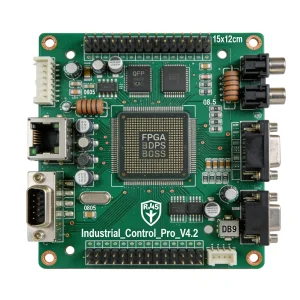
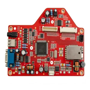

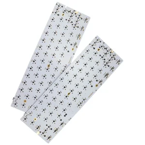
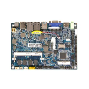

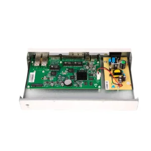
Straight engineering and sourcing answers addressing high-density interconnects, lead-times, MOQ flexibilities, and quality audits.
We utilize high-precision laser-cut electropolished or nano-coated stencils with customized aperture geometries. Solder paste volume is inspected 100% via 3D Solder Paste Inspection (SPI) before pick-and-place. Following multi-zone nitrogen reflow soldering, assemblies pass through 3D Automated Optical Inspection (AOI) and 3D Automated X-ray Inspection (AXI) to verify voiding levels are kept well below 10%, meeting IPC-A-610 Class 3 standards.
No. We do not enforce any minimum order quantities (No MOQ). Our production cells are partitioned into rapid-prototyping NPI (New Product Introduction) lines and high-throughput continuous manufacturing lines. This architecture empowers hardware engineering teams to order 5 to 50 prototype verification boards and seamlessly ramp to tens of thousands of production units on identical SMT feeders and reflow thermal profiles.
Our procurement team utilizes direct ERP integration with global authorized franchised distributors and semiconductor foundries. When a component enters EOL or extended lead times, our component engineering team proposes functional pin-compatible alternate part numbers (Form-Fit-Function equivalents) and executes DFM impact evaluations for client approval before order release.
To provide a binding technical proposal and comprehensive DFM report within 24 hours, we require: (1) ODB++ data or RS-274X Gerber files with drill specifications, (2) Bill of Materials (BOM) in Excel with clear Manufacturer Part Numbers (MPNs) and designators, (3) Centroid / Pick-and-Place file with rotation coordinates, and (4) Fabrication drawing specifying stack-up, impedance tolerances, surface finish (ENIG, ENEPIG, Immersion Silver), and solder mask requirements.
Our Bao'an facility operates two dedicated testing workshops equipped with customizable In-Circuit Test (ICT) bed-of-nails fixtures, Flying Probe testers, high-temperature dynamic burn-in chambers (-40°C to +125°C), high-voltage dielectric withstand testers, RF spectrum analyzers, and automated firmware flashing stations running customer-supplied diagnostic scripts.
Partner with Shenzhen's premier IATF 16949, ISO 13485, and ISO 9001 certified EMS provider. From prototype DFM validation to full volume box-build production, our engineering teams are standing by.
