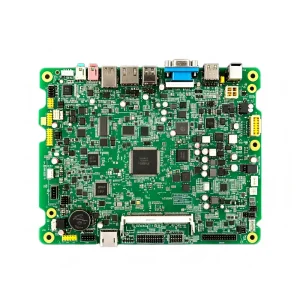
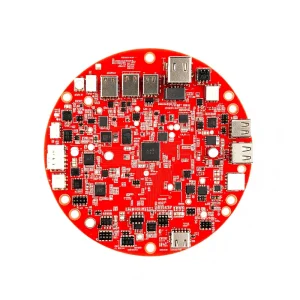
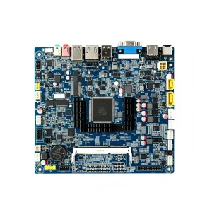
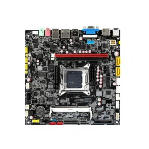
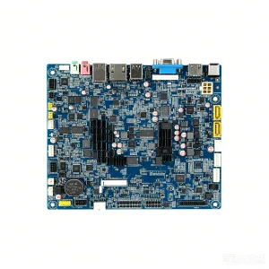
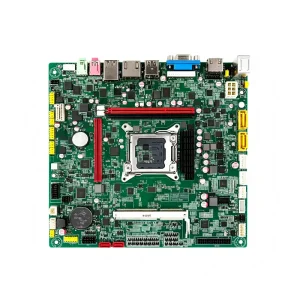
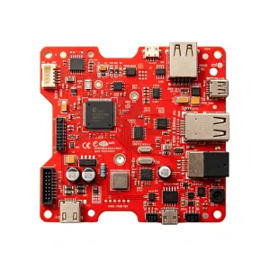
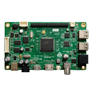
Explore our core turnkey communication PCB manufacturing platforms engineered to withstand extreme thermal, RF, and mechanical stresses.
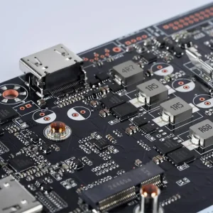
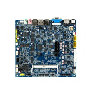
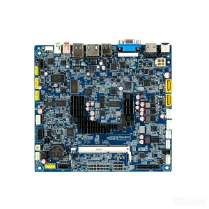
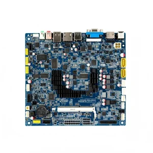
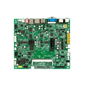
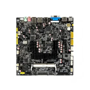
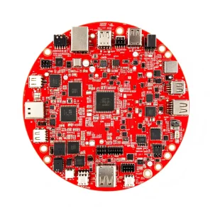
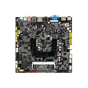
Strategic analysis of procurement demands, high-speed signal integrity engineering, and resilient supply chain mitigation.
In modern telecommunications hardware architecture, the demand for Communication PCB Assembly Factories has transformed from standard electronic manufacturing services (EMS) into deep-tier engineering collaboration. As global telecoms transition from 5G Standalone (SA) configurations toward pre-6G terahertz experiments and high-throughput optical switches, the tolerance margins for insertion loss, cross-talk, thermal dissipation, and parasitic impedance have dropped to near-zero thresholds.
Global Original Equipment Manufacturers (OEMs) and cloud hyperscalers today face a bifurcated challenge: sourcing hardware that simultaneously guarantees sustained dielectric performance across 24/7 mission-critical operations, while ensuring bulletproof lifecycle tracking to combat chip obsolescence and regulatory geopolitical shifts.
Precise handling of low-loss PTFE and hydrocarbon ceramics (Rogers, Taconic, Megtron 6/7/8) with controlled copper tooth profiles to mitigate skin effect losses at frequencies exceeding 40GHz.
Rigorous Backdrilling (stub length < 0.2mm), microvia aspect ratio control, differential pair impedance matching within ±5%, and comprehensive Time-Domain Reflectometry (TDR) validation.
Advanced fine-pitch Ball Grid Array (BGA) placement (down to 0.35mm pitch), Package-on-Package (PoP), and ultra-miniature 01005 / 008004 chip passive soldering under strict nitrogen convection reflow.
Architecting modular PCBA frameworks tailored to distinct network topologies, transmission environments, and power footprints.
Massive backplane assemblies supporting up to 56+ layer multi-layer structures, handling thermal wattages over 400W via embedded copper coin and vapor-chamber heatsink integration.
Active Antenna Unit (AAU) and Remote Radio Unit (RRU) PCBA assemblies optimized for outdoor IP67 hermetic sealing, thermal cycling (-40°C to +105°C), and lightning surge suppression.
High-precision optical transceiver packaging (QSFP-DD, OSFP) operating at 400G/800G, demanding ultra-low flux residue, nitrogen die placement, and strict golden-wire bonding controls.
Hardware-level encrypted firewall and gateway PCBA systems featuring tamper-detection mesh routing, secure cryptoprocessor assembly, and conformal coating against industrial aerosols.
The manufacturing capabilities required to sustain the convergence of Artificial Intelligence clusters and optical fabric scaling.
Meeting telecommunications regulatory requirements across North America, the European Union, APAC, and emerging territories.
Uncompromising compliance for mission-critical networking hardware where downtime is unacceptable, ensuring barrel copper integrity > 1 mil.
Every single reel, silicon wafer lot, and solder paste jar is laser-tracked to the board serial number via Industry 4.0 MES/ERP pipelines.
Complete lead-free assembly processes maintaining full material declaration sheets and halocarbon compliance for international customs verification.
Clear answers to complex technical and sourcing inquiries faced by networking hardware designers and procurement specialists.
Complete the procurement cycle with our high-reliability optical line terminals, wireless modules, and edge accelerators.