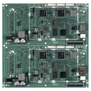
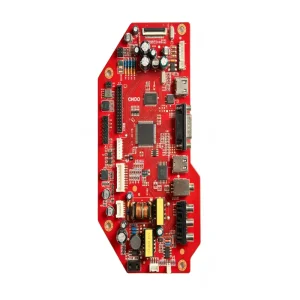
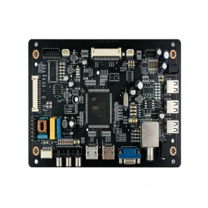
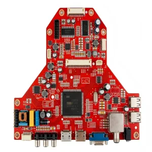
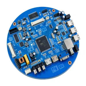
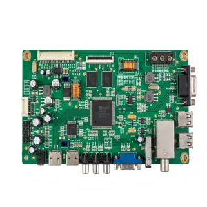
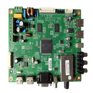
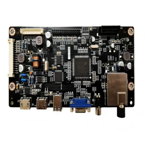
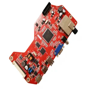
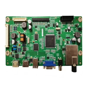
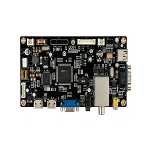
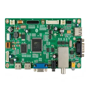
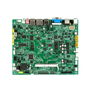
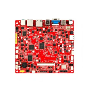
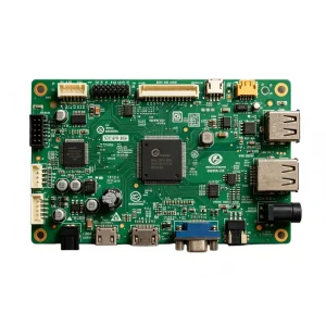
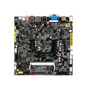
Industrial-grade printed circuit board assemblies engineered for home automation hubs, multi-sensor nodes, voice command devices, and smart displays.
Consumer demands are shifting beyond standalone Wi-Fi switches to unified, hyper-reliable, ultra-low-power ambient computing environments.
The convergence toward the Matter standard mandates sophisticated multi-radio RF layouts. Designers must co-locate Wi-Fi 6, Thread/Zigbee (IEEE 802.15.4), and Bluetooth Low Energy (BLE 5.3) on miniaturized multi-layer rigid-flex boards without cross-talk or degraded TRP/TIS sensitivity.
Smart home nodes now run micro-neural networks directly at the edge—executing wake-word listening, computer vision, and facial biometrics without latency. This necessitates tight power architectures handling sub-milliamp sleep cycles and instant 1A peak bursts.
Regulatory frameworks such as the EU Cyber Resilience Act (CRA) and FCC U.S. Cyber Trust Mark necessitate hardware root-of-trust (RoT) microchips, secure cryptoprocessors, and automated firmware flashing protocols directly within the SMT cleanroom.
Tier-1 smart device vendors, commercial building automation integrators, and OEM brands encounter critical supply chain bottlenecks when scaling connected hardware.
Frequent MCU, RF module, and discrete silicon obsolescence disrupts product lifecycles. Turnkey manufacturers must possess deep engineering acumen to propose drop-in pin-compatible alternates (Second-Source Strategy) without invalidating regulatory certifications.
Smart in-wall dimmer switches and high-voltage motor controllers operate in confined junction boxes without forced-air convective cooling. Efficient PCBA design demands 2oz–4oz heavy copper layers, thermal vias directly under MOSFETs, and high-Tg FR4 substrates.
Transitioning from quick-turn prototype builds to mass volume demands automated Design for Manufacturability (DFM) audits: solder paste aperture profiling, shadow-effect avoidance during reflow, and high-speed pick-and-place fiducial mapping.
How modern intelligent manufacturing plants in the Pearl River Delta achieve lightning-fast lead times without compromising IPC Class III reliability standards.
Every single reel of SMD passives and every semiconductor BGA is scanned upon receiving into our automated storage towers. Line operators maintain barcode-locked batch tracking ensuring every assembled board can be audited down to reel lot and operator station.
Preventing solder bridging and cold solder joints before thermal reflow: 100% 3D Solder Paste Inspection (SPI), high-resolution Koh Young inline AOI for passive alignment, and automated transmission X-Ray inspection (AXI) for hidden BGA/QFN solder voiding (<10%).
Under one 10,000+ m² dust-free roof: precision precision automated selective conformal coating lines protect outdoor and bathroom IoT devices from condensation, followed by full final mechanical enclosure snapping, ultrasonic welding, and drop-ship carton packaging.
Different application verticals require unique component selections, board layer stack-ups, and harsh-environment stress tolerances.
High-accuracy analog-front-end (AFE) circuits on smart thermostat boards measure sub-degree Celsius variations. Relays and Triac circuits in smart plugs handle high in-rush currents (16A inductive) with surge protection exceeding UL 60730 and IEC 61058 safety clearances.
Smart camera and video doorbell PCBA arrays integrate MIPI CSI high-speed differential pairs, HDR image signal processors (ISPs), and dual-band Wi-Fi. Our automated placement handles high pin-count BGA packages down to 0.4mm pitch with zero solder shorts.
Electronic door lock PCB assemblies combine ultra-low power capacitive touch keypads, secure NFC interfaces, motorized latch drivers, and Bluetooth mesh radios. Engineered for continuous vibration resilience and long-term coin-cell battery efficiency.
A granular look at our machinery tolerances, layer capabilities, and testing apparatus calibrated for connected home hardware.
| Assembly Scope | Turnkey Electronic Manufacturing Services (SMT, DIP Through-Hole, Mixed Assembly, Mechanical Box Build) |
|---|---|
| Component Placement Min. Size | 01005 (0402 metric), Fine-Pitch BGA/CSP down to 0.35mm pitch, QFN down to 0.4mm pitch, WLCSP |
| Supported PCB Substrates | FR-4 (Standard & High-Tg 170°C+), Rogers, Aluminum base, Rigid-Flex, Polyimide Flex, Halogen-Free |
| Layer Stack Count | 1 to 32 Layers (Blind & Buried Vias, Microvias, HDI Any-Layer Interconnect) |
| Inspection & Quality Systems | Koh Young 3D SPI, Mirtec 3D AOI, Dage 160kV Inline X-Ray (AXI), In-Circuit Testing (ICT), Flying Probe, FCT |
| RF & Wireless Calibration | Automated RF shielded box testing for Wi-Fi 6, Zigbee, BLE 5.3, Thread, Z-Wave, Sub-1GHz RF TRP/TIS analysis |
| Protective Processing | Nordson Automated Selective Conformal Coating (Acrylic, Silicone, Polyurethane), Underfill, Ultrasonic Potting |
| Certifications Held | IATF 16949 (Automotive), ISO 9001:2015, ISO 13485:2016 (Medical), ISO 14001, RoHS, REACH, UL compliant |
High-reliability switch controllers, smart illumination PCBA modules, motion detectors, and outdoor surveillance hardware.
Direct answers from our senior SMT process and RF engineers regarding DFM reviews, testing matrices, and scaling production.