Certified under IATF 16949 and ISO 13485 standards, our specialized surface-mount and mixed-technology assembly lines produce high-density, mission-grade circuit assemblies with verified solder joint integrity.
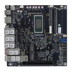
OEM High Quality Automotive PCBA Factory PCB Housing Service Double Side PCBA Factories, Factory
View Specifications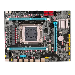
China Computer PCBA Factory Electronic Contract Assembly High Quality PCB Assembly Factories, Factory
View Specifications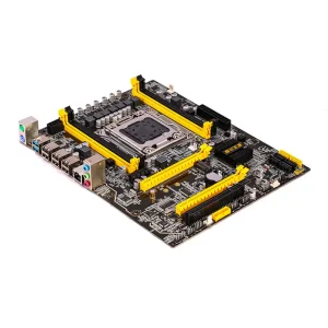
High-Quality Industrial control PCB Assembly--STHL Manufacturer, Service
View Specifications
OEM Automation Equipment PCBA Assembly Factories, Factory
View Specifications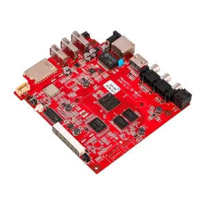
High-Quality Robots Printed Circuit Board Assembly (PCBA): The Neural Core of Precise Robotics-1 Service, Factories
View Specifications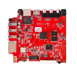
OEM Monitoring Systems PCBA Assembly Manufacturers, Factory
View Specifications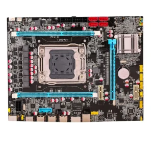
OEM Sensors PCBA Assembly Manufacturer, Factory
View Specifications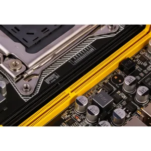
High-Quality Drilling Equipment PCBA Assembly Manufacturer, Manufacturers
View SpecificationsModern electronic systems require an unprecedented convergence of high-density interconnection (HDI), thermal endurance, signal integrity, and supply chain transparency across worldwide commercial frontiers.
Western OEMs in high-stakes sectors such as automotive electrification, medical diagnostics, and robotic automation demand uncompromising traceability. The integration of IPC-A-610 Class 3 workmanship with rigorous Advanced Product Quality Planning (APQP) has shifted supplier evaluations from purely cost-driven bids to comprehensive lifecycle reliability, Design for Manufacturability (DFM) support, and supply chain accountability.
The expansion of smart metering, micro-inverters, and environmental IoT monitoring requires micro-miniaturized electronic assemblies. Factories must routinely handle 01005 passive components, high-pin-count Ball Grid Arrays (BGAs) with 0.35mm pitch, and ultra-thin flexible and rigid-flex circuits while maintaining zero defect rates through automated 3D solder paste inspection (SPI) and inline X-ray verification.
Industrial controls, downhole drilling machinery, and heavy equipment elevators encounter persistent thermal cycling (-40°C to +125°C), moisture condensation, and corrosive airborne contaminants. Modern PCBA application manufacturers must deploy automated conformal coating, epoxy potting, and extensive Burn-in Screening to eliminate infant mortality and guarantee uninterrupted field uptime.
Rooted in Bao’an, Shenzhen—the global epicenter of electronics fabrication—STHL translates dense regional industrial clustering into accelerated engineering cycles, aggressive BOM cost structures, and unmatched supply chain flexibility.
Within a 50-kilometer radius of our Shenzhen facilities lies the world’s most concentrated supply web for active microcontrollers, passive passives, high-Tg substrates, specialized tooling, and custom precision metal/plastic tooling. This allows our procurement engineering teams to secure genuine, traceable components from authorized distributor pipelines (Digi-Key, Mouser, Arrow, Avnet, and Tier-1 factory-direct suppliers) within hours.
Unlike rigid Western contract manufacturers burdened with inflexible setup windows or high minimum order quantity (MOQ) penalties, our 7 automated high-speed SMT lines and 2 dedicated DIP wave-soldering lines accommodate rapid transitions. Hardware startups and tier-one enterprises can transition seamlessly from 5-unit functional proof-of-concept prototypes to 500,000-unit mass production runs using the exact same manufacturing footprint and ERP/MES tracking.
Over 50 dedicated hardware and process engineers evaluate your bill of materials (BOM) and Gerber Gerber/ODB++ files prior to assembly. We proactively identify single-sourced bottlenecks, recommend high-reliability Pin-to-Pin alternatives for obsolete or long-lead ICs, optimize thermal pad layouts to reduce solder bridge defects, and construct custom testing jigs to lower total landed manufacturing expenditure.
Precision electronics must conform to diverse localized deployment environments, ranging from subsea seismic telemetry and agricultural chemical soils to automotive high-voltage powertrain management.
Governed by zero-defect IATF 16949 standards, our automotive assemblies handle battery management systems (BMS), ADAS radar controller boards, and double-sided power inverter drivers. We utilize heavy-copper FR-4 substrates (up to 4oz copper), ceramic baseplates for rapid heat dissipation, vacuum reflow soldering to minimize solder voiding below 8%, and specialized underfills to absorb high-g road shocks.
Multi-axis collaborative robots and automated guided vehicles (AGVs) depend on neural motor controllers capable of high-frequency pulse-width modulation (PWM) with minimal electromagnetic interference (EMI). Our fabrication integrates buried blind vias, 16+ layer balanced stackups, impedance-controlled trace routing, and selective wave soldering to assure deterministic execution across factory floors.
Deployed in remote agricultural soils, wastewater treatment lagoons, and chemical exhaust stacks, monitoring sensors must continuously sample electrochemical, temperature, and gaseous variables. We formulate silicone- and urethane-based conformal coatings that prevent dendritic silver migration and galvanic corrosion, while calibrating low-power sleep state circuits for 10-year battery operational lifespans.
As silicon architectures shrink and silicon-carbide (SiC) and gallium-nitride (GaN) power topologies mature, electronic contract manufacturing must evolve. Our engineering roadmap addresses emerging miniaturization, high-frequency, and thermal dissipation thresholds.
Higher switching speeds reduce transformer and inductor volume but dramatically increase $dv/dt$ transients. Our future-ready SMT lines leverage high-accuracy automated jet dispensers for thermally conductive dielectric adhesives, ensuring that wide-bandgap transistors interface directly with aluminum-backed or copper-core metal substrate PCBs with thermal resistances under $0.5^\circ\text{C/W}$.
Edge AI microprocessors demand any-layer microvia HDI stacks (laser-drilled via-in-pad copper plating) capable of handling BGA pitches as tight as 0.3mm. By eliminating thermal mismatch strains through low-CTE dielectric materials and specialized vacuum-assisted SMT soldering ovens, we achieve void-free BGA joints verified by 3D Computed Tomography (CT) X-ray imaging.
Moving beyond conventional manual inspection, STHL is implementing real-time machine-vision neural networks across all SMT solder print and pick-and-place stages. By comparing real-time solder meniscus curvature and component skew against thousands of trained defective models, the system autonomously adjusts squeegee pressure and feeder alignments before defects can occur.
Compare empirical contract manufacturing capabilities across critical electronic performance parameters, reflecting our operational Bao'an facility standards.
| Manufacturing Parameter | Standard Commercial EMS | STHL Advanced PCBA Factory Standard | Compliance / Validation Method |
|---|---|---|---|
| Min. SMT Component Size | 0402 / 0201 imperial | 01005 (0402 metric) & 03015 micro-passives | High-Precision Yamaha/Panasonic Pick-and-Place |
| BGA & CSP Fine Pitch Capability | 0.50 mm pitch | 0.30 mm pitch with Micro-Via in Pad | 3D AXI (Automated X-Ray) & Endoscopic Inspection |
| Layer Count & Substrate Types | 1 - 8 Layers (Standard FR-4) | 1 - 64 Layers (HDI, Rigid-Flex, Rogers, Polyimide, Metal Core) | IPC-6012 Class 3 Microsection Analysis |
| Solder Voiding Under Power IC / QFN | < 25% voiding ratio | < 8% voiding ratio (Vacuum Reflow Soldering) | Automated Transmission X-ray Metrology |
| Traceability & MES Logging | Batch/Lot Level Traceability | Unit-Level 2D Barcode Serialization (Component-to-Board) | Real-time MES + ERP Enterprise Tracking |
| Harsh Environment Protection | Optional Manual Spraying | Automated Selective Conformal Coating & Potting | IPC-CC-830B / UL94V-0 Flame Retardance Certified |
| Testing Coverage Depth | Visual Inspection + Power-On | Flying Probe, In-Circuit Test (ICT), FCT, Burn-in, Boundary Scan | Custom Functional Test Fixtures & Firmware Flashing |
Navigating international market certification requires robust procedural discipline. Our manufacturing ecosystems strictly adhere to Tier-1 legal and functional compliance across the United States, European Union, APAC, and South America.
We operate audited quality systems that eliminate cross-contamination and guarantee repeatability. Every production step follows strict SOPs, Statistical Process Control (SPC), Gauge R&R validation, and complete production documentation suitable for direct submission to FDA, CE, and automotive audit registries.
All procured passive components, solder alloys (SAC305 lead-free formulations), fluxes, and chemical coatings conform to EU Directive 2015/863 (RoHS 3) and SVHC list under REACH. Comprehensive ICP testing and Material Declaration Sheets accompany outgoing product shipments to ensure frictionless customs entry.
Hardware security begins at the physical assembly line. We execute bilateral non-disclosure agreements (NDAs) prior to receiving proprietary Gerber or schematic files. During production, offline IC programming cells write encrypted firmware via dedicated security dongles, ensuring binary files are isolated from shared computer networks.
Precision electronics engineered for environmental sampling, infrastructure control, noise telemetries, and municipal water monitoring. Retaining full design intent and high thermal stability.
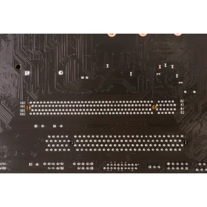
China Elevators PCBA Assembly Service, Factories
View Specifications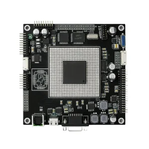
High-Quality Exhaust Gas Monitoring System PCB Assembly Manufacturers, Factory
View Specifications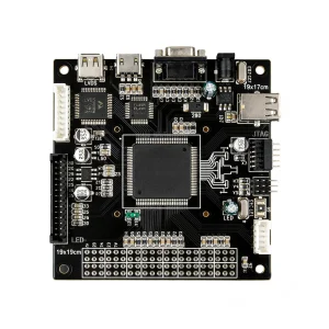
High-Quality Temperature and Humidity Recorder PCB Assembly Service, Factory
View Specifications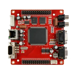
OEM Noise Monitoring Equipment PCB Assembly Manufacturer, Service
View Specifications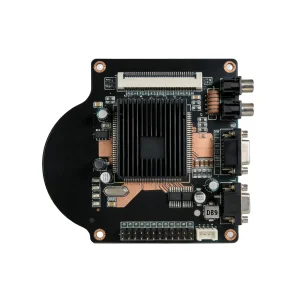
China Soil Detector PCB Assembly Manufacturers, Factory
View Specifications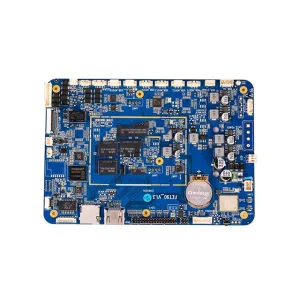
OEM Water Quality Detector PCB Assembly Manufacturer, Service
View Specifications
OEM Air Quality Monitor PCB Assembly Manufacturer, Factories
View Specifications
OEM Wastewater Monitoring Equipment PCB Assembly Manufacturers, Factory
View SpecificationsAnswers to critical engineering questions regarding solder reliability, DFM file preparation, counterfeit component mitigation, and factory qualification.
Counterfeit avoidance is rooted in our ISO 9001 and IATF 16949 incoming material control protocols. STHL sources directly from original component manufacturers (OCMs) or authorized franchised distributors including Digi-Key, Mouser, Arrow, and Avnet. For hard-to-find or legacy parts sourced through secondary tier-one brokers, components pass rigorous in-house physical lab checks: decapsulation die verification, X-ray leadframe inspection, solderability testing, and acetone surface marking wipe tests.
To generate an engineering review and itemized quote within 24 hours, our team requires: (1) Gerber RS-274X or ODB++ fabrication data; (2) A consolidated Bill of Materials (BOM) in Excel format with complete manufacturer part numbers (MPNs), reference designators, package footprints, and designated approved alternatives; (3) Pick-and-Place centroid files (X, Y, rotation, layer); and (4) Detailed functional testing guidelines or acceptance drawings where applicable.
Yes. Our facility operates 7 high-speed SMT surface-mount lines alongside 2 dedicated Dual-Wave and Selective Soldering DIP lines. Whether your design requires fine-pitch BGAs on the top layer, heavy transformers on the bottom, or mixed THT connectors that cannot withstand reflow oven temperatures, we design custom titanium solder pallets for selective wave soldering to achieve consistent joint fillets without heat damaging neighboring SMT passives.
Bottom-terminated components (BTCs) such as BGAs, CSPs, and leadless QFNs cannot be validated via standard optical AOI. We incorporate inline 3D Automated X-ray Inspection (AXI) capable of micro-focus slicing. This inspects for solder bridging, micro-voiding percentage against IPC-A-610 Class 3 thresholds (typically under 10%), ball coplanarity, and excessive solder ball distortion caused by non-uniform thermal reflow expansion.
We maintain a strict No-MOQ policy. We recognize that commercial hardware validation requires rapid prototyping batches (e.g., 5, 25, or 100 units) to verify electrical functionality, enclosure clearances, and environmental resilience before committing capital to tooling or massive inventory. Prototype orders run across the identical high-precision SMT equipment used for volume scaling, assuring direct correlation from pilot batches to mass production.
Before project files are transmitted, our sales and engineering management execute comprehensive bilateral non-disclosure agreements. Digital files reside on permission-controlled intranet servers isolated from external webs. When projects demand on-line microcontroller firmware flashing, our programming stations utilize offline dedicated programmer pods, and all finished PCBA subassemblies undergo automated read-protection bit lock verification before carton packaging.
Submit your Gerber archives and Bill of Materials for an exhaustive Design for Manufacturability (DFM) assessment. Our senior hardware engineers will review your BOM structure, identify obsolete components, and optimize your assembly workflow for superior yield and cost efficiency.
