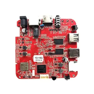
Direct manufacturing solutions engineered across high-frequency telecommunications, heavy-load power electronics, and automotive mission-critical control modules.
The rapid rise of Silicon Carbide (SiC) and Gallium Nitride (GaN) semiconductors has pushed conventional organic substrates (FR-4, polyimide) beyond their physical boundaries. Thermal failure, dielectric breakdown, and coefficient of thermal expansion (CTE) mismatches dictate a structural migration to ceramic-based circuit architectures.
Modern power modules routinely operate at power densities exceeding 100 W/cm². Standard FR-4, with a thermal conductivity of merely 0.3 W/m·K, acts as a heat insulator. In comparison, Alumina (Al₂O₃) provides 24–30 W/m·K and Aluminum Nitride (AlN) delivers 170–230 W/m·K, dissipating heat passively without bulky active heatsinks.
Silicon dies exhibit a CTE of ~3.2–3.5 ppm/K. FR-4 expands at 14–17 ppm/K, causing significant shear strain on solder joints during high-cycle power swings. Ceramic substrates exhibit matched CTE curves (4.5–7 ppm/K), dramatically eliminating micro-cracking and boosting solder joint reliability across thermal excursions from -55°C to +175°C.
Ceramics offer high breakdown voltages (>15 kV/mm), volume resistivities over 10¹⁴ Ω·cm, and extraordinarily low dielectric loss tangents (tan δ < 0.001 at 10 GHz). This prevents signal distortion and phase delays, establishing ceramic circuit boards as the preeminent standard for millimeter-wave radar and sub-6GHz 5G base stations.
Selecting the correct metallization architecture is critical for matching circuit density, mechanical pull-strength, and current carrying capabilities. Our Shenzhen facility manages automated processing lines across four core substrate disciplines.
Leveraging semiconductor thin-film vacuum sputtering and lithography. Achieves ultra-fine traces (<20 µm line/space), smooth surface finishes (Ra < 0.3 µm), and vertical copper-filled vias. Ideal for high-density multi-chip modules (MCM) and optical transceivers.
Pure copper foil fused directly to Al₂O₃ or AlN in a high-temperature eutectic furnace (1065°C). Delivers heavy copper layers (0.1mm–0.8mm) with high peel strengths (>40 N/cm), ideal for high-current IGBT switches, motor drives, and solar inverters.
Utilizing titanium-activated braze alloys to bond thick copper plates onto Silicon Nitride (Si₃N₄) substrates. Si₃N₄ AMB achieves over 800 MPa bending strength and extraordinary fracture toughness for high-stress electric vehicle (EV) traction inverters.
Multi-layered ceramic tapes integrated with internal conductor channels, co-fired below 900°C (LTCC) or at 1600°C (HTCC). Enables embedded passive components (resistors, inductors) and fully hermetic packaging for aerospace avionics and defense sensors.
Definitive physical and geometric tolerances for production validation and Design-For-Manufacturability (DFM) verification.
| Performance Characteristic | Alumina (Al₂O₃: 96% - 99.6%) | Aluminum Nitride (AlN) | Silicon Nitride (Si₃N₄ - AMB) |
|---|---|---|---|
| Thermal Conductivity (W/m·K) | 24 – 30 | 170 – 230 | 90 – 100 |
| Coefficient of Thermal Expansion (ppm/K) | 6.8 – 7.2 | 4.5 – 4.7 | 2.6 – 3.2 |
| Dielectric Constant (1 MHz) | 9.5 – 9.8 | 8.6 – 8.9 | 8.0 – 8.5 |
| Dielectric Loss (tan δ @ 10 GHz) | 1 × 10⁻⁴ | 4 × 10⁻⁴ | 5 × 10⁻³ |
| Bending / Flexural Strength (MPa) | 350 – 450 | 320 – 400 | > 800 (Ultra High Toughness) |
| Surface Finish Metallization | ENIG (Electroless Ni / Immersion Au), ENEPIG, Direct Immersion Silver, Thick Bare Copper | ||
| Standard Thickness Options | 0.25mm, 0.38mm, 0.50mm, 0.635mm, 1.0mm, 1.5mm, 2.0mm (Custom slicing available) | ||
Founded in 2006, Shenzhen STHL Electronics operates over 10,000 m² of ESD-controlled cleanrooms equipped with precision Yamaha & Panasonic high-speed SMT placement systems capable of 01005 component positioning and void-free vacuum reflow soldering.
Void formation under large-format power dies on ceramic substrates drastically degrades thermal pathways. Our inline vacuum-assisted reflow soldering reduces interface voiding rates below 3%, outperforming IPC Class 3 automotive performance criteria.
Dual inline 3D AOI complemented by Nordson Dage High-Resolution 3D X-Ray Inspection ensures solder joint integrity, micro-crack prevention in brittle ceramic matrixes, and precision alignment of fine-pitch wire bonding pads.
Every ceramic substrate, solder chemistry lot, and surface mount component is logged via barcode tracking across our MES workflow, ensuring complete audit transparency for aerospace, military, and medical deployments.
Navigating cross-border electronic hardware production requires rigorous intellectual property safeguards, supply chain resilience, and environmental compliance verified by accredited third-party auditing institutions.
All fabricated ceramic PCBA assemblies adhere strictly to RoHS 3 (EU 2015/863) and REACH (EC 1907/2006) directives. Our processes run halogen-free and conflict-mineral compliant lines under registered ISO 14001 environmental frameworks.
We execute legally binding Non-Disclosure Agreements (NDAs) prior to receiving proprietary Gerber, ODB++, or BOM data. Engineering designs are isolated on secure internal air-gapped file systems to preserve IP ownership for overseas clients.
STHL maintains strategic buffer inventories of raw ceramic raw wafers and essential passives. Our direct air/sea logistics channels maintain certified DDP (Delivered Duty Paid) shipping corridors across North America, the European Union, the UK, and the APAC region.
Real-world deployment validation for ceramic printed circuit boards across demanding industrial, automotive, and deep-well environments.
Thermal accumulation quickly degrades optical output in industrial laser cutting heads and medical phototherapy devices. AlN ceramic circuit boards channel heat away directly, ensuring stable wavelength emission and extending diode service lifetimes past 50,000 operational hours.
Petroleum exploration and geothermal energy extraction subject instrumentation to continuous temperatures exceeding +200°C alongside high vibrations. HTCC and thick-film Alumina systems eliminate delamination risks intrinsic to resin boards.
Electric vehicle 800V fast-charging architectures mandate Si₃N₄ AMB power modules. Our ceramic assemblies handle rapid power cycling, short-circuit current surges, and eliminate catastrophic breakdown caused by partial electrical discharges.
CPV systems concentrate solar energy up to 1000 suns onto compact multi-junction photovoltaic cells. Our DBC Al₂O₃ substrates provide the high insulation and thermal throughput necessary to protect cells from instantaneous thermal meltdown.
Anticipating the converging demands of Quantum Computing, Aerospace Propulsion, and Sub-Terahertz Waveguides.
Transitioning beyond traditional DPC capabilities toward photo-imageable thick-film technology and laser direct imaging (LDI) on AlN substrates, enabling ultra-dense bare-die packaging and direct multi-chip flip-chip integration without interposers.
R&D trials in 3D multi-layered HTCC structures integrating hermetically sealed, micro-channel vapor chambers directly within the ceramic core, achieving localized effective thermal conductivities exceeding 1,000 W/m·K.
Development of synthetic CVD diamond coated onto AlN and Silicon Nitride matrixes. Engineered specifically for next-generation defense RF radar heads, offering unmatched thermal conductivities upwards of 1,500 W/m·K.
Direct answers to the critical technical and supply-chain inquiries fielded by our application engineering department.
Mission-critical manufacturing deployments covering medical life-support systems, industrial backup modules, safety sensor arrays, and grid-scale storage devices.