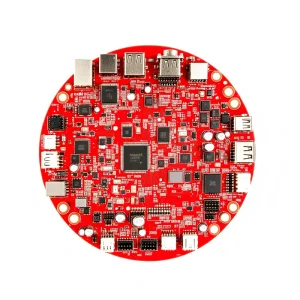
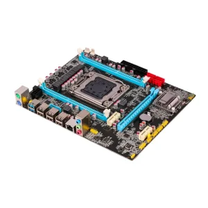
Explore our specialized turnkey assemblies built to withstand elevated junction temperatures, extreme voltage loads, and rigorous thermal shock cycles across automotive and mission-critical installations.
Modern wide-bandgap semiconductors (SiC and GaN) render conventional FR-4 and standard metal-core boards obsolete due to thermal bottlenecks, thermal expansion mismatches, and dielectric breakdown limits.
The industry workhorse offering 96% and 99.6% purity grades. Delivering thermal conductivity between 24 and 35 W/m·K, Alumina provides exceptional mechanical hardness, optimal cost-efficiency, and unmatched chemical corrosion resistance for high-volume automotive sensors and industrial modules.
Engineered for extreme thermal dissipation with figures reaching 170 to 230 W/m·K—nearly 8 times higher than standard alumina. Its thermal expansion coefficient (4.5 ppm/K) closely matches semiconductor dies, preventing shear fatigue in lead-free solder interconnects across massive heat cycles.
Renowned for superior flexural strength (>650 MPa) and fracture toughness (6.5-7.0 MPa·m½). Si₃N₄ withstands extreme mechanical stress and thermal cycling shocks up to 100,000 cycles, establishing it as the benchmark substrate for EV traction inverters and wind energy converters.
| Substrate Parameter | Alumina (Al₂O₃ - 96%) | Aluminum Nitride (AlN) | Silicon Nitride (Si₃N₄) | Standard FR-4 / MCPCB |
|---|---|---|---|---|
| Thermal Conductivity (W/m·K) | 24 - 28 | 170 - 230 | 80 - 90 | 0.3 (FR4) / 1.5 - 3.0 (MCPCB) |
| Dielectric Strength (kV/mm) | 15 - 18 | >15 | >20 | 15 (Organic breakdown >130°C) |
| CTE (ppm/K, 20-300°C) | 6.8 - 7.2 | 4.5 - 4.7 | 3.0 - 3.4 | 14 - 17 (Z-axis mismatch) |
| Bending / Flexural Strength (MPa) | 380 | 350 | >700 | N/A (Delaminates) |
| Fabrication Metallization | DBC, DPC, Thick Film | DBC, DPC, AMB | Active Metal Brazing (AMB) | Electrodeposited Foil Bonded |
Shenzhen STHL Electronics provides an agile, end-to-end manufacturing footprint that eliminates intermediate tier-2 vendor margins and minimizes technical friction from substrate laser drilling to certified EMS fulfillment.
Immediate local access to premium ceramic powders, ultra-flat sintered green sheets, and oxygen-free high-conductivity (OFHC) copper foils reduces procurement lead times from months to business days.
Laser via drilling, DPC magnetron sputtering, DBC nitrogen tunnel sintering, precision photolithography, and ENIG/ENEPIG surface plating are executed 100% under our single roof without external contractor latency.
High-speed diamond tooling, in-house direct imaging (LDI), and scalable automated production lines slash engineering NRE and per-unit BOM costs compared to European or North American boutique substrate providers.
From single-piece proof-of-concept samples delivered within 5-7 business days to multi-million mass production batches backed by 7 dedicated SMT lines and zero minimum order quantity (No MOQ) mandates.
Western procurement directors and Tier-1 automotive integrators operate under zero-defect imperatives. Our factory operational matrix bridges overseas compliance expectations with native engineering execution.
Complete serialization from incoming laser-scanned raw ceramic lot codes to post-reflow automated optical inspection (AOI) and 3D X-ray (AXI) void verification, assuring failure isolation across 15+ years.
Comprehensive Non-Disclosure Agreements precede any data transmission. Schematics, gerber databases, laser routing coordinates, and BOM configurations are stored in air-gapped, encrypted networks.
Full accreditation including IATF 16949 (Automotive), ISO 13485 (Medical Devices), ISO 9001 (Quality Systems), ISO 14001 (Environmental), and full RoHS/REACH compliance documentation for border clearance.
As power density boundaries expand across electric mobility, industrial robotics, deep-space avionics, and high-frequency 5G/6G RF circuits, ceramic-based PCBA serves as the foundational substrate enabling continuous operation.
Silicon Carbide (SiC) MOSFET modules, onboard chargers (OBC), DC-DC power stages, and electronic braking (EPB) operating continuously beyond 175°C junction thresholds with zero laminate breakdown.
Massive MIMO antennas, radar transceivers, and millimeter-wave front-ends benefit from low dielectric constants (εr ~ 9.0) and ultra-low dissipation factors (tan δ < 0.001) up to 40+ GHz.
Laser diode arrays, UV-C curing modules, and stage/automotive matrix LED headlamps requiring direct copper trace attachment without intermediate thermal grease layers.
Megawatt-scale central solar inverters and wind-turbine pitch controls subjected to harsh outdoor environmental shifts, moisture ingress, and non-stop operational stress.
Direct technical clarification on ceramic printed circuit board fabrication, metallurgy limits, solder assembly, and project lead times answered by STHL staff engineers.
Direct Bonded Copper (DBC) bonds thick copper foils (100–300μm) directly onto ceramics in a 1065°C nitrogen furnace, ideal for high-current EV inverters. Direct Plated Copper (DPC) utilizes thin-film sputtering and electroplating for fine pitch circuits (trace width/spacing down to 30μm). Active Metal Brazing (AMB) incorporates titanium into brazing alloys, creating superior peel strength on Silicon Nitride (Si₃N₄) for severe thermal shock environments.
Unlike traditional mechanical routing that introduces stress fissures, STHL deploys ultrashort pulse UV and picosecond laser machining platforms. Laser ablation vaporizes the ceramic material with near-zero heat-affected zones (HAZ), preventing micro-fractures during depanelization, drilling of micro-vias, or tight cavity profiling.
Because ceramic substrates do not expand at standard FR-4 rates, high-reliability lead-free alloys such as SAC305, SN100C, or high-melting AuSn (gold-tin) pastes are preferred. SMT reflow profiles require precise preheating ramps (1.5–2°C/sec) to avoid substrate thermal shock, followed by controlled cooling under nitrogen atmospheres.
Yes. We specialize in LTCC (Low Temperature Co-fired Ceramic) and HTCC (High Temperature Co-fired Ceramic) processes that enable up to 40 internal routing layers. Tungsten/molybdenum paste metallization is co-fired with glass-ceramic sheets to embed internal passives, shielding layers, and high-density vertical interconnects.
Engineered for uncompromising stability, our secondary portfolio spans aerospace crew alert interfaces, renewable smart switching, and Class-III medical device electronics.
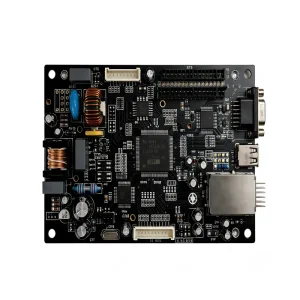
High-Quality Engine Indicating and Crew Alerting System (EICAS) PCBA Assembly--STHL Manufacturer, Factories
Review Feasibility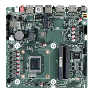
China Energy PCBA Application: Powering the Future of Renewable Energy Manufacturers, Factory
Review Feasibility
China Medical PCBA Application: Precision and Reliability for Healthcare Devices Manufacturer, Factories
Review Feasibility