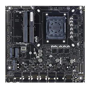
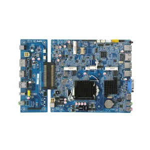
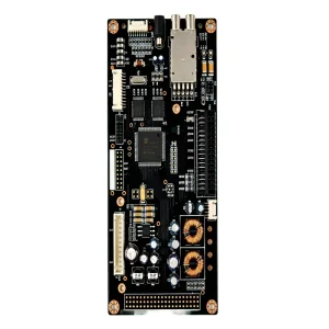
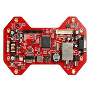
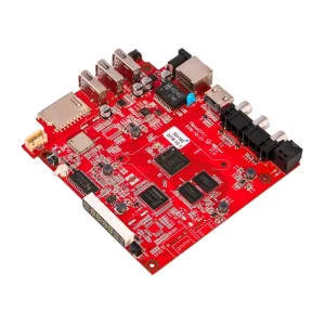
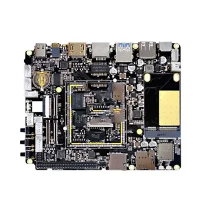
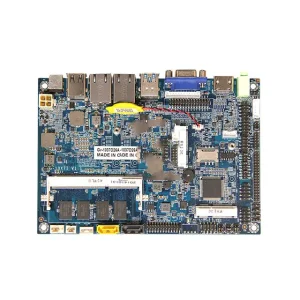
Explore our verified turnkey PCBA implementations across high-frequency radar, aerospace, robotics, e-mobility, and automation sectors manufactured under strict IPC-A-610 Class 3 controls.
Navigating technical complexity, geopolitical diversification, and total cost of ownership (TCO) in Tier-1 electronics contract manufacturing.
In modern high-velocity hardware engineering, printed circuit board assembly (PCBA) has transformed from a mere assembly transaction into a highly interdependent engineering discipline. International technology enterprises across North America, the European Union, the United Kingdom, Japan, and Australia face compounding procurement challenges: volatile passive and active component lead times, the rapid proliferation of high-density interconnect (HDI) requirements, fine-pitch ball grid arrays (BGA) down to 0.35 mm pitch, and strict regulatory standards including UL, CE, FCC, RoHS, and REACH. Selecting a manufacturing partner in China is no longer merely a cost-reduction exercise; it is an indispensable strategic alignment with the world’s densest electronics ecosystem.
Shenzhen, often termed the hardware Silicon Valley of the world, offers an unmatched concentration of raw material fabricators, semiconductor distributor networks, tooling facilities, and specialized surface-mount technology (SMT) infrastructure. A complete design cycle—from prototype revision verification, Design for Manufacturability (DFM) audits, Bill of Materials (BOM) cross-referencing, bare board lamination to volume SMT placement and in-circuit functional testing—can be executed within a fraction of the lead time demanded by regional vendors elsewhere. However, securing this systemic speed requires an accountable partner operating under rigid international quality protocols.
How Tier-1 engineering protocols de-risk component counterfeiting, solder joint fatigue, impedance mismatches, and multi-vendor operational friction.
Uncontrolled open-market broker sourcing accounts for over 78% of catastrophic field failures due to counterfeit silicon, aged solder terminations, or salvaged ICs. STHL enforces 100% franchised distributor procurement (Arrow, Avnet, Digi-Key, Mouser, Farnell, WPG) backed by certificate of analysis (CoA), incoming lot inspection, and x-ray package verification.
Over 40% of standard Gerber packages contain thermal shadow hazards, insufficient solder dams, pad-to-trace necking, or component spacing violations that precipitate solder bridging. Our team of 50+ engineers executes algorithmic DFM and DFA verification prior to any tooling, drastically shortening revision cycles and avoiding costly board scrap.
Disaggregating bare PCB fabrication, component sourcing, SMT placement, cable assembly, and final testing across disparate contractors introduces blame games during yields drop. STHL takes full ownership under one ISO 9001, IATF 16949, and ISO 13485 framework, delivering unified warranties and transparent ERP/MES real-time order tracking.
Tailored manufacturing workflows developed specifically for the stringent thermal, mechanical, and signal integrity requirements of leading industries.
IPC-A-610 Class 3 compliant assembly incorporating heavy copper traces, ceramic substrates, conformal polyurethane or silicone coating, and rigorous thermal cycling (-55°C to +125°C) for avionics, satellites, and high-altitude flight controllers.
Engineered under IATF 16949 certification to satisfy zero-defect mandates. Tailored for battery management systems (BMS), high-power inverter modules, millimeter-wave radar sensors, and ADAS autopilot controllers handling extreme vibration and current spikes.
Manufactured under ISO 13485 quality protocols with full device history records (DHR). Supporting ventilators, patient telemetry monitors, syringe infusion pumps, and portable diagnostic analyzers requiring strict bio-burden and electromagnetic immunity.
Ultra-dense multi-layer circuit boards with embedded microvias, high-speed differential pairs (PCIe Gen 4/5, USB4, 10GbE), and FPGA/NPU processor integration. Dedicated functional burn-in and automated optical test fixtures guarantee round-the-clock uptime.
Comprehensive engineering benchmarks established across STHL’s 7 automated SMT lines, DIP workshops, and functional test bays in Bao'an, Shenzhen.
| Manufacturing Parameter | Production Capability Specification | Advanced / Custom Capabilities | Quality Verification Instrument |
|---|---|---|---|
| SMT Component Packaging | 01005 (0402 metric), 0201, 0402, 0603, QFN, DFN, TSOP | 0.3mm ultra-fine pitch micro-BGA, PoP (Package-on-Package) | 3D Solder Paste Inspection (SPI) + Offline 3D AOI |
| BGA Placement Accuracy | ±0.025 mm alignment accuracy; Pitch ≥ 0.35 mm | X-Ray inspection of voiding ratio < 8% (IPC Class 3) | High-resolution X-ray inspection (2D/3D AXI) |
| Bare Board Layer Count | 1 to 32 Layers (Rigid FR-4, Rigid-Flex, Aluminum IMS) | Up to 48 Layers; HDI 1+N+1 to Any-Layer HDI via fill | Flying probe test + Micro-section metallurgical analysis |
| Substrate Materials | Standard FR-4, High-Tg (TG170/180), Halogen-free | Rogers 4350B, Taconic, PTFE, Polyimide Flex, Ceramic | Dielectric Breakdown Tester & TGA thermal stability |
| Solder Reflow & Soldering | 10-zone Nitrogen (N2) forced convection reflow ovens | Selective soldering, Nitrogen wave soldering for mixed tech | KIC thermal profiling systems on every product revision |
| Value-Added Secondary Ops | Conformal coating (Acrylic, Silicone, Polyurethane), Potting | Laser marking, IC bare die flashing, Wire harnessing, Enclosure | Automated conformal coating UV thickness measurement |
Preserving project profitability and delivery timetables through active lifecycle surveillance and cross-continent supplier redundancy.
When unexpected factory shutdowns or multi-month allocation bottlenecks freeze microcontroller or power management IC shipments, our electrical engineering team formulates form-fit-function (FFF) drop-in replacements. Every proposed alternate undergoes rigorous validation of electrical transients, input/output characteristics, and thermal dissipation margins prior to client sign-off.
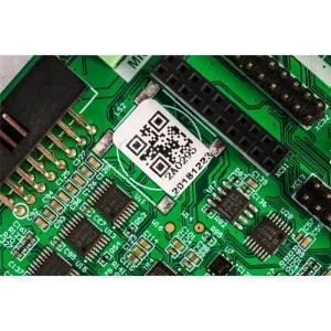
Every reel, tray, and tube received into STHL’s humidity-controlled, ESD-shielded warehouse is tagged with an internalized UID barcode. This barcode binds components directly to ERP material master records and Shop Floor Manufacturing Execution Systems (MES), establishing 100% granular trace-back from the finished end-device box to the silicon wafer batch.
We respect client intellectual property, consignment preferences, and strategic supplier contracts. STHL accommodates 100% turnkey sourcing, partial consignment (where the OEM supplies programmed master MCUs/FPGAs or custom ASIC packages), or complete consignment kit handling with equal rigor in incoming material control.
Deploying deterministic inspection fixtures to ensure every delivered PCBA operates flawlessly throughout its full anticipated operational life.
Over 65% of SMT anomalies originate at the solder paste printing phase. Inline 3D SPI measures paste volume, pad coverage, height, and coplanarity across every PCB before component placement, catching deviations in real-time.
High-speed telecentric cameras inspect tombstoning, polarity, component orientation, and billboarding. For leadless packages (BGA, QFN, LGA), non-destructive 2D/3D X-Ray guarantees zero solder ball bridging or internal pad voiding.
In-Circuit Testing checks each trace for opens, shorts, resistance, capacitance, and active diode behavior. Bed-of-nails fixtures are custom-fabricated for high-volume orders, while flying probe is mobilized for rapid, fixtureless prototypes.
Boards undergo dynamic load testing, communications bus querying (CAN, RS-485, Ethernet, I2C, SPI), and thermal chamber stress tests under full operating power to weed out early-life component infant mortality.
Aligning factory infrastructure with emerging developments in photonics, silicon carbide (SiC), gallium nitride (GaN), and AI-augmented electronics.
With electric vehicle on-board chargers, solar microinverters, and datacenter PSUs shifting toward Gallium Nitride and Silicon Carbide power stages, switching frequencies surpass hundreds of kilohertz with elevated thermal density. STHL is advancing specialized vacuum reflow soldering and sintered silver paste technologies that eliminate micro-voids, elevating thermal conductivity and mechanical shear strength.
Wearables, drone navigation pods, and handheld ultrasound instruments demand extreme miniaturization beyond conventional discrete 0201 soldering. Our engineering research initiatives center around embedded passive components buried directly inside PCB prepreg cores, reducing outer loop parasitic inductances, freeing surface real estate, and enhancing electromagnetic compliance.
Transitioning from post-defect inspection to proactive in-line parameter correction. By feeding continuous optical measurements from solder paste inspection (SPI) and placement vision cameras into neural network models, our upcoming smart factory iterations dynamically modulate squeegee pressure, print velocity, and pick offsets, achieving true six-sigma manufacturing capability.
Safeguarding engineering designs, firmware payloads, and legal compliance across North American, European, and regional territories.
Every engineering review begins under mutual Non-Disclosure Agreements (NDAs). Design archives are partitioned across enterprise intranets with role-based cryptographic permissions. Flashing workstations can utilize client-encrypted binaries and secure hardware tokens, guaranteeing proprietary firmware cannot be extracted, cloned, or redistributed.
STHL operates under ISO 14001 environmental frameworks and enforces strict lead-free, RoHS 3 (EU 2015/863), and REACH (SVHC) substance restrictions. Solder alloys (SAC305, SN100C) and laminates are independently certified by third-party testing bodies (SGS, TUV) with full documentation for client CE and UL submissions.
Exporting to over 90 countries with complete Incoterms coverage (EXW, FOB, CIF, DDP). Our dedicated customs compliance team manages tariff classification (HS codes), origin declarations, and air/sea expedited shipping via FedEx, DHL, UPS, and ocean freight, avoiding customs holds or unforeseen border surcharges.
A transparent, stage-gated transition model that accelerates time-to-market while safeguarding mechanical and electrical integrity.
Client submits Gerber RS-274X/ODB++, structured BOM, and Pick & Place centroid data. STHL engineers return an exhaustive DFM analysis within 24 hours detailing thermal reliefs, clearance checks, and component availability.
Rapid setup tooling and SMT stencil fabrication. A controlled pilot batch (5 to 50 pcs) is manufactured, complete with first-article inspection (FAI) reports, reflow profile logs, and functional verification for engineering sign-off.
Transition to continuous high-speed placement lines. Integration of automated laser solder printing, high-speed dual-beam placers, multi-zone nitrogen reflow, wave soldering, and automated optical/X-ray verification.
Conformal coating, injection molding enclosure assembly, ultrasonic welding, wire harness integration, custom retail/industrial ESD packaging, and international export under unified shipment tracking.
In-depth technical, commercial, and operational clarifications addressing the specific concerns of overseas hardware engineering managers.
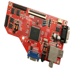
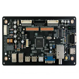
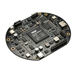
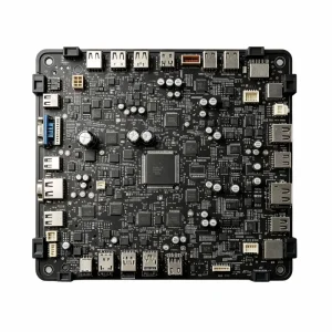
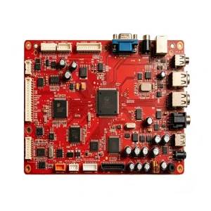
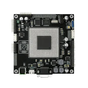
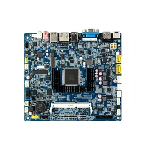
Proven PCB assemblies deployed globally in medical respiratory equipment, automotive navigation systems, high-speed optical transceivers, and power networks.

Connect directly with our senior hardware and DFM engineers in Shenzhen. We sign mutual Non-Disclosure Agreements (NDAs) prior to file intake and deliver full DFM assessments and transparent quotation matrices within 24 hours.
