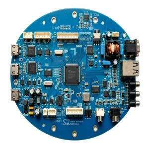
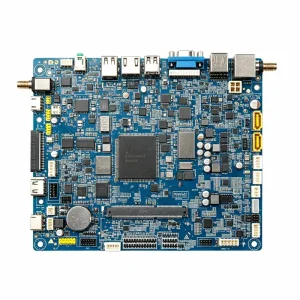
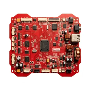
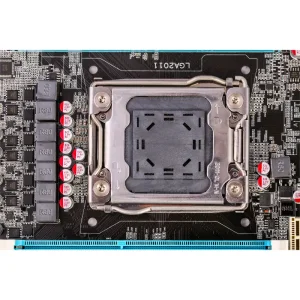
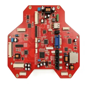
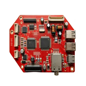
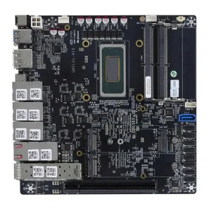
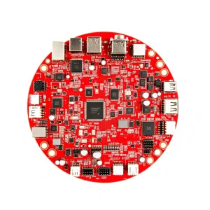
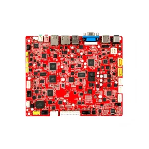
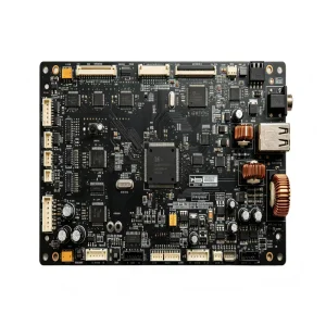
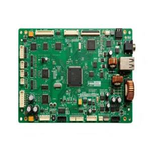
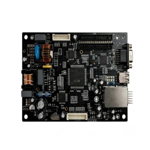
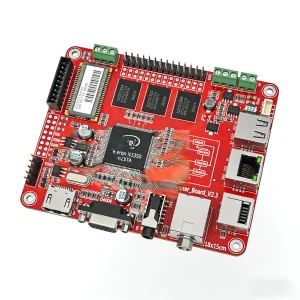
Explore precision-manufactured PCBA units engineered for extreme operational stability across automotive, telecommunications, energy storage, and diagnostic medical equipment.
From simple double-sided board etching to high-density multi-layer interconnects (HDI), embedded component substrates, and automated turnkey electronic manufacturing systems.
Modern electronic engineering requires an unbroken digital bridge between raw Gerber CAD files and robotic surface-mount machines. Chinese PCBA manufacturers have transitioned from low-cost board houses into fully automated EMS hubs that execute DFM verification, rapid multi-layer fabrication, active component procurement, and automated in-circuit validation inside a centralized MES workflow.
By enforcing IATF 16949 and ISO 13485 operating frameworks, advanced factories utilize serialized 2D laser matrix codes etched onto every bare laminate. This assigns a unique digital ledger to every solder joint, component batch, reflow thermal curve, and 3D AOI inspection scan, ensuring uncompromising compliance for automotive and aerospace sectors.
Before copper deposition begins, factory application engineers execute algorithmic DFM and DFA checks. This critical step evaluates trace aspect ratios, annular rings, solder mask clearances, thermal dissipation pads, and bill-of-materials (BOM) obsolescence, saving international OEMs hundreds of thousands of dollars in tooling spins and redesign delays.
How the world's most concentrated microelectronics industrial ecosystem delivers unprecedented component availability, pricing leverage, and cycle acceleration.
The electronics cluster in Shenzhen’s Bao'an and surrounding Pearl River Delta regions houses an incomparable ecosystem of certified semiconductor distributors, authorized passive component brokers, and specialty raw laminate suppliers. Through direct integration with over 100 global authorized channels—including Arrow, Avnet, Digi-Key, Mouser, and top domestic fabless vendors—our factory maintains instant visibility into over 500,000 verified part numbers. This eliminates extended procurement lead times, avoids production line downtime, and provides resilient buffers against volatile international spot markets.
Traditional overseas manufacturers often segment quick-turn prototype shops from high-volume automated factories. In Shenzhen, the continuum is seamless. A prototype PCB layout can undergo photochemical laser direct imaging (LDI), automated wet-chemical processing, multi-layer vacuum lamination, surface treatment (ENIG, OSP, Immersion Silver), and high-speed pick-and-place assembly within 24 to 48 hours. Once functional bench testing confirms hardware viability, identical fabrication stack-ups and machine programs transfer directly to high-throughput lines without requiring line requalification or redesign cycles.
| Procurement & Manufacturing Metric | Typical Western Regional Facility | Tier-1 China Factory (STHL Ecosystem) | Operational Strategic Advantage |
|---|---|---|---|
| BOM Sourcing Turnaround | 2 to 4 Weeks (Subject to Stockists) | 24 to 72 Hours (Shenzhen Direct Channels) | Shortened product launch cycles by 65% |
| Bare Board Layer Capabilities | 1 to 16 Layers Standard | 1 to 64 Layers HDI, Rigid-Flex, Thick Copper | Enables ultra-dense compute & sensor nodes |
| Minimum Order Restrictions (MOQ) | Strict MOQ or Excessive Engineering NRE | No MOQ (From 1 Prototype to 1,000,000 Units) | Zero inventory overhang for early-stage pilots |
| Tooling & SMT Stencil Fabrication | 3 to 7 Days (Outsourced Third-Party) | Same-Day High-Precision Laser Cut Stencils | Rapid engineering revisions and trial runs |
| BGA Pitch Placement Threshold | Down to 0.4mm pitch standard | Down to 0.3mm pitch with 01005 ultra-fine passives | Supports cutting-edge automotive and mobile SoCs |
A rigorous seven-stage quality framework bridging raw dielectric copper substrates to encapsulated, firmware-flashed systems ready for global deployment.
Every engineering release is parsed through automated Valor CAM platforms. Factory layout specialists inspect track width, trace space, drill-to-copper clearances, via-in-pad plating, and thermal pad geometry to prevent solder bridging and tombstoning prior to production sign-off.
Utilizing high-Tg FR4, polyimide flexible layers, Rogers high-frequency laminates, or metal-core aluminum boards. Processes include micro-via laser drilling, blind/buried via fills, electrolytic acid copper plating, and precise impedance matching within ±5% tolerances.
Solder deposition is maintained using fully automatic screen printers with closed-loop squeegee pressure. Immediately downstream, inline 3D Solder Paste Inspection (SPI) evaluates volume, area, height, and registration to eliminate 70% of potential surface-mount defects.
Seven automated modular SMT lines equipped with dual-beam placement heads position complex Ball Grid Arrays (BGA), Quad Flat No-leads (QFN), and passives down to 01005 sizing. Wave and selective soldering stations handle rugged power connectors and through-hole relays.
Post-reflow quality verification uses 3D Automated Optical Inspection (AOI) to detect tombstoning, polarity inversions, and insufficient fillets. High-resolution transmission X-Ray inspection penetratively checks hidden BGA ball coplanarity, void ratios, and inner-layer wet bonding.
Beyond optical scans, bare PCBA boards undergo bed-of-nails In-Circuit Testing (ICT), flying probe checks, and tailored Functional Testing (FCT). Units are powered to operational voltage, flashed with client firmware, and subjected to RF signal calibration and full load simulations.
To resist corrosive environmental elements, boards receive automated robotic selective conformal coating (acrylic, silicone, or polyurethane). Complete mechanical assembly integrates custom CNC housings, injection molded enclosures, wiring harnesses, and final retail packaging.
Strategic purchasing managers evaluate beyond nominal per-unit quotes. Mitigate operational risks, eliminate hidden tariffs, and maximize gross manufacturing margins.
Electronics procurement is constantly challenged by component lifecycle changes, unannounced end-of-life (EOL) notices, and unpredictable allocations. Our factory engineering staff proactively recommends form-fit-function (FFF) second-source alternatives from vetted tier-1 Asian and global manufacturers, frequently yielding 15% to 35% overall BOM cost reductions while maintaining compliance and system stability.
We implement stringent technical confidentiality protections before receiving engineering data. Mutual Non-Disclosure Agreements (NDAs), encrypted off-network CAM workstations, restricted server access, and proprietary firmware flashing protocols ensure that international intellectual property, software binaries, and circuit topologies remain strictly guarded.
True cost equals the acquisition price plus the cost of quality failure. By maintaining a First-Pass Yield (FPY) above 99% and conducting 100% full electrical functional validation in Shenzhen, international OEMs avoid catastrophic ocean freight returns, customer warranty claims, and field recalls that degrade market reputation.
Ensuring your finished hardware meets legal operating benchmarks across North America, the European Union, the United Kingdom, and Asia-Pacific markets.
Automotive electronics manufacturing standard requiring rigorous advanced product quality planning (APQP), FMEA risk registers, and strict error-proofing across all sub-tier suppliers.
Medical device quality framework ensuring lot-level component traceability, ESD-controlled cleanrooms, and risk management documentation for patient-connected diagnostics.
Certified inline visual and structural inspection standards defining precision criteria for solder joints, barrel fill percentages, BGA voids, and surface cleanliness.
Strict non-hazardous substance governance verifying lead-free assembly (melting profile >217°C) and UL flame retardancy certifications across all bare laminate grades.
Engineered to withstand extreme environments, electrical stress, continuous thermal cycling, and stringent regulatory demands.
In-vehicle computers, Telematics Control Boxes (T-Boxes), Battery Management Systems (BMS), and On-board Chargers (OBC) require resilient substrates capable of handling mechanical vibration, thermal shock from -40°C to +125°C, and heavy copper current paths with rigorous potting and conformal coatings.
Commercial photovoltaic inverters, micro-inverters, and high-capacity battery energy storage system (BESS) controllers demand high creepage and clearance distances, heavy copper foil (up to 6oz), reinforced galvanic isolation, and surge suppression across critical switching stages.
Medical CT scanners, dialysis monitor controllers, and handheld ultrasound units demand extreme signal fidelity, low-noise multi-layer analog routing, high-density HDI design with micro-vias, and cleanroom assembly under strict ISO 13485 production controls.
DIN-rail switched-mode power supplies, Programmable Logic Controllers (PLCs), and edge IoT gateways deployed in noisy factory environments utilize transient voltage protection, optically coupled isolated inputs, and thick FR4 multi-layer boards tested for 24/7/365 uninterrupted operation.
Power over Ethernet (PoE) switches, enterprise VoIP communications hardware, and industrial routers utilize controlled differential impedance matching (100Ω differential, 50Ω single-ended) and low-loss dielectric laminates to ensure zero packet loss and low signal attenuation.
Aviation subsystems, Cockpit Voice Recorders (CVR), and Engine Indicating and Crew Alerting Systems (EICAS) are produced to IPC Class 3 standards, undergoing environmental stress screening (ESS), thermal cycling, and high-frequency vibration testing.
The transformation of EMS factories through AI-driven optical validation, embedded passive substrates, and sustainable green manufacturing standards.
Deep-learning algorithmic visual inspection engines are replacing traditional rule-based AOI systems. By training neural networks on millions of solder joint variations, factories detect micro-bridging, solder balling, and minute component tilts without triggering false positive alerts.
As wearable electronics, edge AI sensors, and mobile hardware compress internal volumes, manufacturing processes are shifting toward modified Semi-Additive Processes (mSAP). This facilitates ultra-fine trace and space geometries below 30μm/30μm, approaching silicon packaging densities.
Leading Chinese EMS factories are implementing green manufacturing programs to comply with global ESG mandates. Initiatives include closed-loop micro-etch copper reclamation, low-temperature soldering alloys to reduce reflow power consumption, and 100% recyclable halogen-free base materials.
Direct, technical answers addressing file preparation, testing capabilities, lead times, and quality governance for global hardware developers.
To deliver an accurate, binding DFM review and quotation within 24 hours, our engineering staff requires: (1) RS-274X or ODB++ Gerber files with layer stack-up definitions; (2) Detailed Bill of Materials (BOM) in Excel format with manufacturer part numbers, descriptions, reference designators, and approved alternative vendors; (3) Pick-and-Place (Centroid / XY coordinates) file; (4) Fabrication and assembly drawings showing mechanical clearances; (5) Written functional testing specifications.
Our quality assurance department maintains a zero-tolerance anti-counterfeiting program. We procure strictly through original semiconductor component manufacturers or their authorized tier-1 franchised distributors. For spot-market purchases of critical allocated ICs, incoming components pass through our analytical inspection laboratory, undergoing decapsulation testing, X-Ray die inspection, solderability verification, and marking permanence testing.
Quick-turn prototype bare boards can be fabricated in 24 to 48 hours. Turnkey prototype assembly—including rapid component procurement, laser stencil cutting, surface mounting, and inspection—is typically delivered in 5 to 7 working days. For standard medium-to-high volume production runs, lead times typically range from 3 to 4 weeks, depending primarily on specific long-lead active semiconductors identified during initial BOM reviews.
Yes. Our automated SMT lines are equipped with advanced multi-camera vision systems capable of placing micro-BGAs down to 0.3mm pitch, ultra-fine-pitch QFNs, and 01005 passive chips. Solder joint integrity beneath leadless components is systematically verified via 3D Automated Optical Inspection (AOI) and industrial multi-axis transmission X-Ray systems to confirm voiding levels remain below 10%.
We do not enforce an MOQ policy. We actively support engineering clients through initial NPI (New Product Introduction), proof-of-concept prototypes, pilot batches of 5 to 50 boards, and seamless expansion into tens or hundreds of thousands of units. This flexibility allows engineering teams to validate circuit revisions on the exact same assembly lines used for mass production.
Firmware flashing protocols are segregated within dedicated, air-gapped programming cells. Software binaries are stored on encrypted, access-restricted local network directories and loaded using automated flash programmers. Flash verification guarantees checksum matching, after which read-protection security bits are set to prevent reverse-engineering before the board leaves our factory.
Certified electronics manufacturing spanning automotive double-sided PCBA, switching and DIN-rail power modules, solar power inverters, and high-reliability aerospace avionics.