Explore production-grade assemblies manufactured under IATF 16949 and ISO 13485 quality protocols, representing seamless transition from bare PCB fabrication to surface-mount execution.
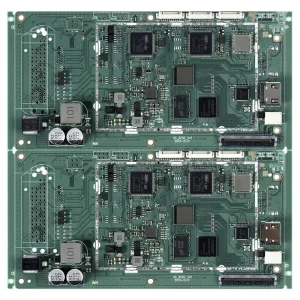
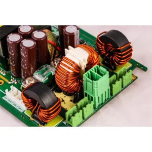
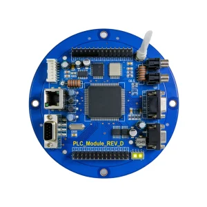
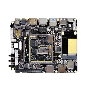
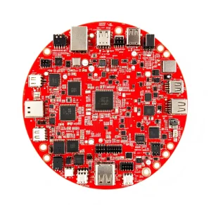
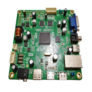
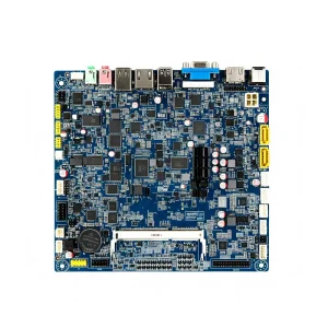
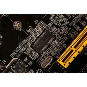
A fundamental structural distinction exists between raw substrate manufacturing and the multifaceted integration of active/passive silicon in fully assembled electronics.
| Differentiating Vector | Bare Printed Circuit Board (PCB) Fabrication | Printed Circuit Board Assembly (PCBA) & EMS |
|---|---|---|
| Physical Definition | A passive mechanical substrate etched with conductive copper traces, vias, dielectric layers, and solder mask to facilitate future electrical interconnections. Contains zero populated silicon chips or discrete passive components. | A fully integrated electro-mechanical sub-assembly featuring functional active chips, microcontrollers, passive components, memory modules, and physical connectors mounted, soldered, and firmware-programmed onto the bare PCB. |
| Core Manufacturing Processes | Photolithography, chemical etching, mechanical/laser via drilling, multilayer lamination, copper electroplating (electrolytic and electroless), solder mask silkscreening, and surface finish application (ENIG, HASL, OSP). | Precision solder paste stencil printing (SPI verification), Surface Mount Technology (SMT) high-speed chip placement, multi-zone reflow oven soldering, Through-Hole Technology (THT/DIP) wave or selective soldering, conformal coating, and enclosure assembly. |
| Primary Failure Modes | Delamination, inner-layer copper micro-cracking, barrel plating separation in vias, impedance mismatches, conductive anodic filament (CAF) formation, and solder mask peeling. | Solder bridging, tombstoning of 0201/01005 passives, BGA voiding, cold solder joints, electrostatic discharge (ESD) silicon breakdown, thermal profiling damage, and component polarity inversions. |
| Quality Standards & Inspection | IPC-A-600 Acceptability of Printed Boards, IPC-6012 rigid board specifications, Flying Probe testing, Automated Optical Inspection (AOI) of inner/outer etch layers, and micro-section thermal shock stress testing. | IPC-A-610 Acceptability of Electronic Assemblies, IPC J-STD-001 soldering requirements, 3D Solder Paste Inspection (SPI), 3D Automated Optical Inspection (AOI), 3D X-ray Inspection (AXI) for BGA/QFN, and In-Circuit Testing (ICT). |
| Supply Chain Dependencies | Raw laminates (FR4, Rogers, Polyimide, Aluminum), copper foil rolls, prepreg sheets, chemical photoresists, and metallic plating chemistries. | Global semiconductor silicon procurement, active ICs, passive reels (MLCC, resistors), electromechanical connectors, flux chemistries, solder alloys (SAC305), and custom firmware code flashing. |
Bare board fabrication focuses primarily on substrate glass transition temperatures (Tg), dielectric constants (Dk), dissipation factors (Df), and coefficients of thermal expansion (CTE) across X, Y, and Z axes. In contrast, PCBA manufacturing requires mastery of dynamic thermal profiling inside 10-to-12 zone reflow ovens.
Assemblers must balance delta-T tolerances to ensure high-mass power inductors reach full eutectic wetting without scorching adjacent ultra-thin BGA silicon substrates or inducing micro-voiding beneath thermal heat pads.
Sourcing engineers frequently conflate DFM disciplines. Bare PCB fabrication requires DFF validation: annular ring ratios, copper-to-edge clearances, drill-aspect ratios, and etch-compensation tolerances.
Conversely, PCBA demands stringent DFA (Design for Assembly) optimization: stencil aperture-to-pad ratios, component keep-out zones for pick-and-place nozzles, shadow effects during wave soldering, fiducial marker placement, and test-point accessibility for automated bed-of-nails in-circuit fixtures.
Walking the factory floor highlights irreconcilable operational infrastructures. Bare PCB facilities represent heavy chemical and mechanical environments with acid copper plating tanks, etching chambers, vacuum hot presses, and cleanroom photolithography rooms.
In stark contrast, a Tier-1 PCBA assembly facility like STHL Electronics in Shenzhen operates Class 100,000 ESD-protected, climate-stabilized cleanrooms equipped with high-speed Yamaha/Panasonic pick-and-place systems, nitrogen-atmosphere reflow ovens, and Automated X-ray Inspection stations.
Why Tier-1 global OEMs converge on China’s Greater Bay Area for integrated PCB fabrication and turnkey assembly services.
Situated in Shenzhen’s Bao’an District, STHL harnesses an unmatched geographical advantage. Over 98% of passive chip resistors, capacitors, standard diodes, microcontrollers, and specialized electromechanical connectors can be sourced, authenticated, and delivered to line feeders within hours.
China-based EMS providers leverage long-term tier-1 distribution agreements with global semiconductor manufacturers (Microchip, STMicroelectronics, TI) alongside audited domestic second-source alternatives. This strategic dual-sourcing architecture protects hardware startups and industrial OEMs from single-point silicon chokeholds.
Supply chain security requires continuous verification. STHL’s incoming material quality control (IQC) protocol integrates decapsulation testing, X-ray leadframe inspection, solderability verification, and acetone wipe marking analysis to guarantee that every component on your BOM is 100% genuine and traceable back to original wafer lots.
When engineering teams contract bare board fabrication to Vendor A and SMT assembly to Vendor B, assembly defects (such as solder de-wetting or micro-via fractures) inevitably spark vendor disputes. A unified China PCBA partner assumes full mechanical, metallurgical, and electrical accountability from Gerber design to final box-build packaging.
As computing workloads transition toward edge AI, automotive autonomy, and ultra-miniaturized smart wearables, PCB fabrication and PCBA assembly are undergoing structural convergence.
Transitioning from traditional mechanical drilling (0.15mm limit) to UV/CO2 laser-drilled microvias (≤0.075mm). Implementing stacked and staggered copper-filled microvias across 10+ layers, enabling ultra-tight 0.35mm BGA pitch fan-outs for compact IoT and computing boards.
Adoption of the Modified Semi-Additive Process (mSAP) enables line width and line spacing (L/S) below 25/25µm. This bridges the physical density gap between traditional rigid circuit boards and silicon wafer-level integrated circuit substrates for portable flagship devices.
Embedding discrete MLCC capacitors, resistors, and silicon dies directly within the inner dielectric layers of the bare PCB. This shortens signal interconnect paths, virtually eliminates parasitic inductance, and maximizes outer surface area for high-pin-count processors.
Executing zero-halogen resin formulations, bio-derived dielectric substrates, and low-temperature bismuth-tin (Sn-Bi) solder alloys to reduce reflow peak temperatures from 245°C down to 170°C, lowering thermal stress and cutting manufacturing energy footprints by up to 35%.
Engineering Directive: STHL Electronics continuously aligns its SMT machinery with miniaturization trends. Our high-precision placement lines support 01005 passive placement, 0.3mm ultra-fine-pitch CSP packaging, and 3D Automated Optical Inspection capable of sub-micron coplanarity validation.
From mission-critical automotive architectures to sensitive medical telemetry, different operating environments dictate custom PCB material stack-ups and PCBA soldering chemistries.
Automotive hardware must endure extreme thermal cycling (-40°C to +125°C), sustained vibration, and aggressive electromagnetic interference.
Medical electronics mandate absolute electrical signal integrity, ultra-low leakage currents, and complete traceability over multi-decade lifecycles.
High-power solar inverters, battery management systems (BMS), and industrial motor drives handle extreme kilowatt surges and continuous high-temperature stress.
A rigorous quality management architecture bridges bare-board fabrication accuracy with high-yield surface mount execution.
Before metal is routed or solder paste applied, STHL’s senior engineering team subjects client Gerbers, BOMs, and centroid coordinates to exhaustive Design for Excellence (DFx) reviews:
Our manufacturing protocols are validated through independent third-party certification audits, verifying standard compliance across every production stage:
Enterprise Resource Planning (ERP) and shop-floor Manufacturing Execution Systems (MES) generate a digital certificate of conformance for every board batch:
Authoritative technical guidance for hardware founders, engineering directors, and procurement leaders evaluating electronics manufacturing partners.
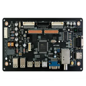
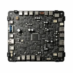
Explore additional mission-critical PCBA modules engineered and assembled in our Shenzhen manufacturing plant, demonstrating robust performance across demanding power and industrial environments.

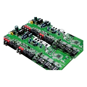
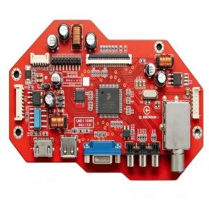
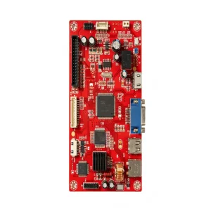
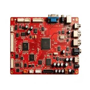

Eliminate multi-vendor friction by unifying bare PCB fabrication and turnkey SMT assembly under one accountable, IATF 16949-certified quality management system.
Send your Gerber files, Bill of Materials (BOM), and Centroid pick-and-place data securely under mutual NDA protection.
Our 50+ staff engineers evaluate your layout for design rules, component availability, pin-pad alignments, and assembly testability.
From rapid prototyping with zero MOQ to continuous mass production, our facility ships tested, fully certified electronics assemblies worldwide.
