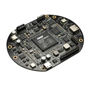
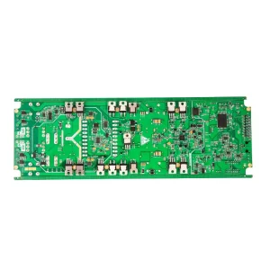
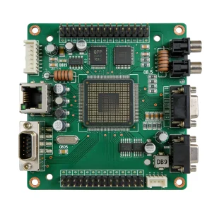
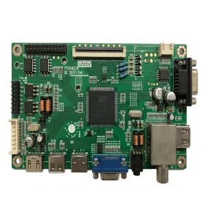
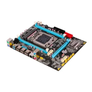
China Electronics Manufacturing Process Manufacturers & Service

A technical blueprint and industrial whitepaper covering turnkey Surface Mount Technology (SMT), high-reliability PCB fabrication, mission-critical component engineering, and global OEM contract manufacturing solutions from Shenzhen, China.

20+
Years EMS Experience
10,000m²
Smart Factory Facility
50+
Senior Process Engineers
13+
Automated SMT & Test Lines
99.5%
On-Time Global Delivery
0-MOQ
Prototyping to Mass Run
Precision Engineering Solutions

Featured Industrial & Commercial PCB Assemblies

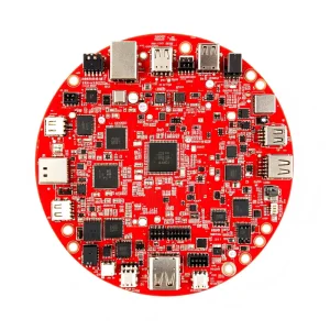
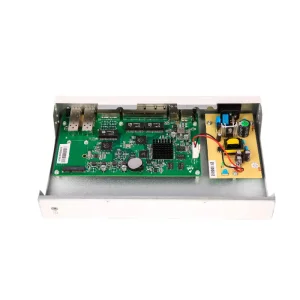
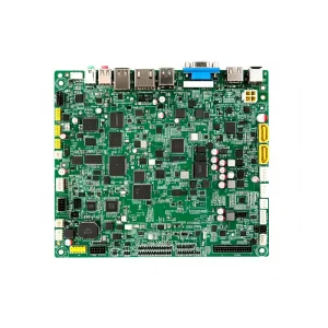
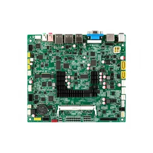
Explore our production-ready electronic modules manufactured to IPC-A-610 Class 2 and Class 3 reliability standards. Engineered with closed-loop process control for demanding international deployments.
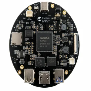
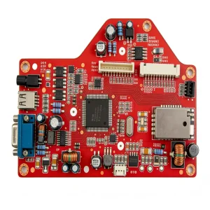
OEM Smoke Detector PCBA Assembly
OEM Smoke Detector PCBA Assembly--STHL Factories, Factory
View Specifications
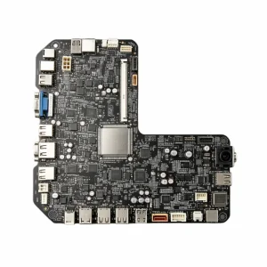
High-Quality Surveillance Camera PCB Assembly
High-Quality Surveillance Camera PCB Assembly Manufacturer, Service
View Specifications
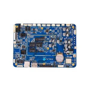
OEM Air Quality Monitor PCBA Assembly
OEM Air Quality Monitor PCBA Assembly--STHL Manufacturer, Factories
View Specifications
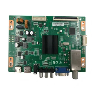
OEM Smart Garage Door Opener PCBA Assembly
OEM Smart Garage Door Opener PCBA Assembly--STHL Manufacturers, Factory
View Specifications
China Camera PCB Assembly
China Camera PCB Assembly PCB Assembly-1 Manufacturers, Factories
View Specifications
Hot-Swappable Power Supply PCB Assembly
High-Quality Hot-Swappable Power Supply PCB Assembly--STHL Service, Factory
View Specifications
OEM Water Quality Detector PCB Assembly
OEM Water Quality Detector PCB Assembly Manufacturer, Service
View Specifications
Power over Ethernet Injector PCB Assembly
OEM Power over Ethernet Injector (PoE Injector) PCB Assembly--STHL Manufacturers, Service
View Specifications
Global Industrial Landscape

The Macro Dynamics of Electronics Manufacturing in China

Over the past two decades, China’s Electronic Manufacturing Services (EMS) industry has transformed from a low-cost contract assembly hub into an integrated global powerhouse characterized by intelligent automated factories, cutting-edge SMT lines, and hyper-responsive supply chain clusters.

Shenzhen’s Hardware Agility

Located at the epicenter of global hardware innovation, Shenzhen offers unprecedented supply chain concentration. Passives, active microcontrollers, multilayer substrates, and custom metal stampings can be sourced and iterated within a 50-kilometer radius, drastically condensing the New Product Introduction (NPI) cycle for overseas innovators.

  • Instant component availability via qualified domestic hubs
  • Accelerated functional prototype assembly within 24 to 72 hours
  • Scalable transition from quick-turn runs to high-volume manufacturing

Resolving Sourcing Bottlenecks

Global tier-1 OEMs and growing hardware start-ups often struggle with fractured supply networks, volatile component availability, and counterfeit risks. An integrated EMS partner delivers direct authorized-distributor access and deep BOM cost-optimization capabilities.

  • Direct procurement relationships with Arrow, Avnet, Digi-Key, and Mouser
  • Proactive Life-Cycle Analysis (EOL / LTB / Obsolete Part mitigation)
  • Certified second-source qualification without sacrificing electrical specs

Rigorous IP & Quality Governance

Overseas hardware enterprises demand institutional-grade IP protection and strict compliance adherence. Operating under international standards ensures that intellectual assets, custom firmware, and proprietary schematics remain impenetrable.

  • Legally vetted Bilateral NDAs before receiving Gerber and BOM packages
  • Audited certifications: IATF 16949, ISO 13485, ISO 9001, ISO 14001
  • Segregated programming servers and encrypted automated test jigs
Engineering Methodology

Comprehensive Electronics Manufacturing Process (EMP) Deep Dive

Precision electronics manufacturing is not merely about mounting components on copper laminates; it is a systematically monitored, zero-defect process requiring micrometer-level calibration across multi-stage production phases.

1. AI-Driven DFM & DFA Verification

Before any tooling commences, experienced engineering personnel subject customer CAD/Gerber packages to rigorous Design for Manufacturability (DFM) and Design for Assembly (DFA) screening. We analyze annular ring margins, thermal relief paths, copper balancing, and component shadow risks for wave or reflow operations.

2. IQC & Traceable Procurement

All raw semiconductors, passive chips, and custom silicon undergo stringent Incoming Quality Control (IQC). We implement reel-level x-ray fluorescence (XRF) inspection to verify RoHS compliance, solderability dipping tests, and electrical capacitance/resistance sampling, backed by lot-level MES barcoding.

3. High-Layer PCB Substrate Fabrication

From standard FR-4 to specialized substrates like Rogers high-frequency laminates, polyimide flex, rigid-flex, and aluminum-core metal clad boards, substrates are built with high-density interconnect (HDI) laser micro-vias, controlled impedance routing (±5%), and electroplated finishes (ENIG, Immersion Silver, OSP).

4. High-Precision SMT & Nitrogen Reflow

Automated paste printing features real-time 3D Solder Paste Inspection (3D-SPI). Modular pick-and-place systems mount ultrafine packages down to 01005 passives, 0.3mm-pitch BGAs, and QFNs. Reflow occurs in multi-zone convection ovens blanketed with pure Nitrogen (N2) to eliminate intermetallic oxidation.

5. Multi-Angle 3D AOI & HD X-Ray (AXI)

Every soldered assembly passes inline 3D Automated Optical Inspection (AOI) to eliminate tombstoning, polarity inversions, and insufficient fillets. For hidden ball grid arrays (BGA), quad-flat no-leads (QFN), and power FETs, high-resolution Automated X-Ray Inspection (AXI) guarantees voiding ratios below 15%.

6. Conformal Coating, Box Build & FCT

For harsh environments, automated selective conformal coating (acrylic, silicone, or polyurethane) provides moisture, salt-spray, and chemical barriers. Finished PCBA boards are routed into full electro-mechanical enclosures (Box Build) and validated via automated Functional Circuit Testing (FCT) jigs.

End-to-End Applications

Macro Industry Sector Solutions & Process Customization

Different mission profiles demand distinct assembly protocols. Our manufacturing facilities configure production parameters, thermal profiles, and inspection checkpoints tailored specifically to the operational stresses of end-market sectors.

Automotive & EV

Adhering to IATF 16949 quality guidelines, we produce on-board chargers, battery management systems (BMS), and ADAS sub-assemblies tested to withstand harsh temperature cyclings from -40°C to +125°C.

Medical & Life Sciences

Compliant with ISO 13485 standards, our clean-room facilities manufacture surgical ventilators, wearable clinical monitors, and laboratory automated fluid diagnostic assemblies with 100% full-lot traceability.

Industrial IoT & Power

Heavy-copper substrates, high-voltage galvanic isolation, and conformal potting for hot-swappable industrial supplies, PoE injectors, explosion-proof monitors, and utility gas alarms operating in volatile environments.

Smart Connected Infrastructure

Wireless networking routers, high-resolution optical surveillance cameras, smoke alarms, and IoT garage controllers integrated with impedance-matched RF circuitry and tuned antennas.

Engineering Thresholds

Manufacturing Capability & SMT Tolerance Parameters

Direct from our factory floor: an authoritative parameter overview for design engineers, procurement specialists, and quality auditors validating production alignment prior to RFQ submission.

Manufacturing Dimension Standard Baseline Specification Advanced / High-Density Capability
PCB Layer Count 1 – 16 Layers (Rigid FR-4) Up to 48 Layers (HDI Anylayer, Rigid-Flex, Blind/Buried Vias)
Min. Passive Component Size 0402 Imperial (1.0 × 0.5 mm) 01005 Imperial (0.4 × 0.2 mm) / 03015 Metric
Fine-Pitch IC & BGA Ball Pitch 0.5 mm Ball Pitch / 0.4 mm Lead Pitch 0.3 mm Micro-BGA, Ultra-fine QFN, PoP (Package-on-Package)
Placement Accuracy & Speed ±0.035 mm @ 3 Sigma ±0.015 mm @ 3 Sigma (High-Precision Optical Alignment)
Board Dimensional Range 50 × 50 mm min. to 450 × 350 mm max. Up to 1200 × 500 mm (Long-Board LED / Backlight Strips)
Board Thickness Range 0.4 mm – 3.2 mm 0.15 mm (Ultra-thin flex) to 6.0 mm (Heavy-duty backplanes)
Finished Copper Weight 1 oz – 2 oz Up to 10 oz Heavy Copper (High-Current Inverters & EV Chargers)
Soldering Atmospheric Environment Forced Air Convection (Lead-Free / SAC305) Pure Nitrogen (N2) Tunnel Inhabitation (Residue < 500ppm O2)
Non-Destructive Joint Metrology Automated 3D-AOI + Manual Sampling High-Resolution 3D Computed Tomography AXI & Flying Probe
Quality & Industry Standards IPC-A-610 Class 2, ISO 9001 IPC-A-610 Class 3, IATF 16949, ISO 13485, ISO 14001
Next-Generation Roadmap

Technology Roadmap & Future Outlook (2025–2030)

As semiconductor lithography shrinks and edge AI processors push board-level thermal limits, electronics manufacturing processes must evolve to support high thermal dissipation, heterogeneous multi-die modules, and green production cycles.

Heterogeneous Packaging & SiP

System-in-Package (SiP) and embedded passive substrates are blurring traditional boundaries between component packaging and surface mounting. Our advanced lines are adapting to assemble bare silicon die, flip chips, and micro-sensors directly within organic cavities.

  • Integration of micro-underfill dispensing for thermal resilience
  • Embedded passive component integration reducing layout footprint by 40%

Closed-Loop AI Smart Manufacturing

Industry 4.0 digital twin environments are linking 3D-SPI printers directly with high-speed mounters and reflow ovens. Instant feedback loops automatically correct solder stencil offsets and nozzle pressures before soldering defects can physically manifest.

  • Autonomous machine vision classifying solder joints in real time
  • MES-connected predictive maintenance preventing feeder mispicks

Green Chemistry & Low-Carbon Assembly

Meeting European and North American carbon-neutral regulations requires total supply-chain sustainability. We are introducing low-temperature solder (LTS) alloys, halogen-free laminates, and zero-VOC water-soluble flux cleaning technologies.

  • Low-temperature Bi-Sn alloys cutting thermal energy usage by 35%
  • Comprehensive ISO 14001 environmental auditing & RoHS/REACH verification
Global Reliability

Localized Customer Support, Global Logistics & Compliance Assurance

International trade demands smooth operational bridges. We eliminate friction for overseas procurement officers through bilingual engineering liaison desks, transparent shipping logistics, and bulletproof trade documentation.

Dedicated English Engineering Desk

Direct interaction with senior English-speaking DFM and process engineers prevents communicative ambiguity. Engineering queries (EQ) are resolved within 24 hours, ensuring your technical intent is mirrored on the assembly line.

Flexible DDP / FOB Logistics

Whether handling air shipments to Frankfurt and Chicago or ocean freight to Santos and Auckland, our freight network handles customs clearance, harmonized tariff codes (HS code classification), and door-to-door DDP arrangements seamlessly.

MES End-to-End Serialization

Every board features laser-etched 2D DataMatrix serialization. Customers can trace individual passive component batches, reflow oven temperature profiles, and final automated functional test logs years after product deployment.

Procurement Knowledgebase

Frequently Asked Questions (FAQ)

In-depth technical answers addressing critical sourcing considerations, quality protocols, component security, and contract delivery expectations.

What documentation package is required to obtain an accurate turnkey PCBA quotation?
To provide an itemized, transparent turnkey quotation, we require: (1) Standard Gerber files (RS-274X or ODB++ format) including all copper, solder mask, silkscreen, and drill layers; (2) A comprehensive Bill of Materials (BOM) in Excel format with distinct columns for Item Number, Reference Designator, Manufacturer Part Number (MPN), Brand Name, Component Description, Package Footprint, and Quantity per Board; (3) Pick-and-Place Centroid coordinate data (.txt or .csv); and (4) Assembly drawings outlining conformal coating keep-out zones and custom testing criteria.
How does your factory prevent counterfeit or re-balled active components from entering the line?
We adhere strictly to anti-counterfeit standard AS5553. First, our procurement team sources directly from certified franchised distributors (Arrow, Avnet, DigiKey, Mouser) or original semiconductor manufacturers. Second, our Incoming Quality Control (IQC) station conducts high-magnification optical inspection to detect surface markings or sanding artifacts, X-ray inspection to confirm die presence and internal wire-bonding integrity, and XRF material analysis to ensure pin finish authenticity.
Can you accommodate mixed orders with low volumes and prototype iterations without an MOQ penalty?
Yes. We enforce a zero Minimum Order Quantity (0-MOQ) policy. We maintain dedicated quick-turn SMT lines tailored specifically for rapid NPI prototypes (1 to 50 pieces) without demanding setup penalties. Once your prototype design passes electrical and environmental testing, the exact engineering settings, solder profiles, and feeder setups are seamlessly scaled onto our mass production lines.
What functional and reliability tests are executed prior to final packing?
Depending on application criticality, our testing suite incorporates: (1) Inline 3D-AOI optical defect review; (2) Automated X-ray (AXI) for BGA solder joint void evaluation; (3) In-Circuit Testing (ICT) or Flying Probe testing to verify netlist continuity and passive values; (4) Custom Functional Testing (FCT) via customer-specified test firmware and automated bed-of-nails fixtures; (5) Burn-In and Thermal Cycling under full voltage load; and (6) Dielectric Withstand / Hi-Pot safety tests.
What is the standard turnaround lead time for complete turnkey PCBA orders?
Turnkey lead times depend on active component lead times. For rapid prototyping where components are readily in stock, our quick-turn PCB fabrication and assembly cycle takes 3 to 7 working days. For standard production volumes, lead times typically range from 3 to 4 weeks, during which we execute bare PCB fabrication, component sourcing, SMT assembly, automated testing, and box build integration concurrently.
How does your factory manage design file revisions and Engineering Change Orders (ECO)?
Engineering Change Orders are managed through our centralized MES and ERP system under strict revision controls. Upon receiving an ECO, previous Gerber and BOM iterations are instantly frozen on our floor terminals. Our engineering team reviews the delta, updates pick-and-place centroids, verifies stencil aperture impacts, and generates a formal revision audit trail that requires mutual engineering sign-off prior to re-initiating production.
Specialized Implementations

Advanced System Builds & Harsh-Environment Electronics

Explore our specialized sub-assemblies built for extreme thermal tolerances, medical-grade patient isolation, automotive charging conditions, and hazardous industrial atmospheres.

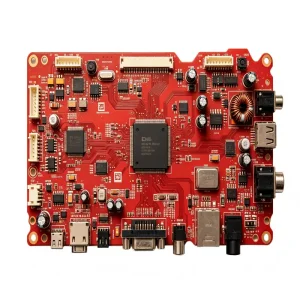
OEM Explosion-proof Equipment PCB Assembly
OEM Explosion-proof Equipment PCB Assembly--STHL Manufacturers, Service
View Specifications
OEM Ventilator PCB Assembly
OEM Ventilator PCB Assembly--STHL Manufacturer, Manufacturers
View Specifications
High-Quality Gas Leak Alarm PCB Assembly
High-Quality Gas Leak Alarm PCB Assembly--STHL Service, Factories
View Specifications
Laboratory Automation Equipment PCB Assembly
China Laboratory Automation Equipment PCB Assembly--STHL Service, Factory
View Specifications
NEV On-board Charging Equipment PCB Assembly
China New Energy Vehicle On-board Charging Equipment PCB Assembly Manufacturer, Manufacturers
View Specifications
OEM LED TV Backlight Strip PCB Assembly
OEM LED TV Backlight Strip PCB Assembly--STHL Manufacturers, Factory
View Specifications
Health Monitoring Devices PCBA Assembly
China Health Monitoring Devices (such as smart bracelets) PCBA Assembly--STHL Manufacturers, Factory
View Specifications
Wireless Network Router PCB Assembly
China Wireless Network Router PCB Assembly--STHL Service, Factory
View Specifications

Ready to Optimize Your Electronics Manufacturing Chain?

Submit your Gerber files and Bill of Materials today for an institutional-grade DFM feasibility assessment, component cost-reduction evaluation, and formal production quotation within 24 hours.