Explore production-grade SMT and mixed-technology assemblies produced in Shenzhen for global OEM engineering teams.
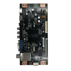


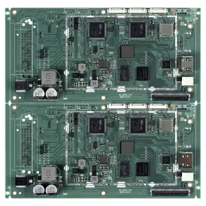
The global electronics contract manufacturing environment has transitioned from sheer labor-cost arbitrage to high-velocity, software-orchestrated agility. In Shenzhen and the greater Greater Bay Area (GBA), the synergy between raw laminate manufacturers, passive component vendors, silicon distributors, and advanced SMT providers forms an unmatched ecosystem capable of accelerating NPI (New Product Introduction) cycles by over 60% compared to Western counterparts.
Founded in 2006, Shenzhen STHL Electronics Co., Ltd. operates at the center of this transformation. As an enterprise operating under IATF 16949 (automotive) and ISO 13485 (medical) certifications, STHL integrates complete end-to-end transparency: linking component provenance to multi-zone automated optical inspection (AOI) and closed-loop SPI platforms.
Supply Chain Redundancy: STHL maintains verified access to over 500,000 distinct components via authorized agreements with tier-one global distributors (Arrow, Avnet, Digi-Key, Mouser) and domestic primary fabs, hedging overseas buyers against volatile lead times and single-point-of-failure disruptions.
Strategic challenges in automotive powertrain electrification, AIoT micro-packaging, and harsh-environment telemetry require systemic upgrades across the assembly landscape.
With consumer and portable medical systems demanding footprint minimization, SMT lines must reliably position 01005 passives and ultra-fine-pitch CSPs (down to 0.35mm ball pitch) under strictly controlled solder paste volumes.
Secure hardware demands verified non-disclosure protocols and encrypted IC flashing architectures. Modern Chinese factories provide dedicated, physically isolated programming environments that protect intellectual property.
The acceleration of GaN and SiC semiconductors creates elevated thermal densities. Board manufacturers must implement copper coin embedding, heavy copper stackups, and ceramic hybrid substrates with optimized void-free vacuum soldering.
Zero-defect manufacturing relies on real-time process monitoring, statistical process control, and serialized batch traceability.
Automated Solder Paste Inspection evaluates deposit volume, height, area, and bridging before component placement, adjusting stencil alignment automatically.
Lead-free thermal profiles exceed standard 217°C liquidus thresholds with tightly maintained peak temperatures (235°C–245°C) to prevent delta-T stress on sensitive ICs.
High-resolution optical and X-Ray inspection detects hidden solder defects, BGA head-in-pillow anomalies, and internal micro-voiding beneath thermal heat sinks.
Laser-etched QR codes on every bare board tie component reels, pick-and-place feeders, reflow timestamps, and functional test data into a single queryable record.
A structured 7-stage quality gating protocol safeguards design intent from pre-production DFM review through to box-build logistics.
Pre-assembly evaluation of Gerber, BOM, and centroid files under strict NDA to eliminate clearance bottlenecks before stencil laser etching.
Incoming inspection of silicon, actives, and passives through certified franchised agents, including reel verification and anti-counterfeit testing.
High-speed surface-mount placement with nitrogen reflow, followed by selective wave or manual through-hole soldering compliant with IPC-A-610 Class 2/3.
In-circuit testing (ICT), custom firmware flashing, functional validation, selective conformal coating, and enclosure assembly ready for deployment.
STHL operates 7 advanced SMT lines, 2 specialized DIP/THT lines, 2 dedicated functional test cells, and 2 box-build assembly lines inside a modern 10,000+ m² Shenzhen facility.
| Compliance Standards | IATF 16949, ISO 13485, ISO 9001, ISO 14001, IPC-A-610 Class 2 & 3 |
|---|---|
| Minimum Component Size | 01005 (0402 metric), BGA ball pitch down to 0.35mm, CSP, QFN |
| Board Thickness & Size | 0.2mm to 4.5mm thickness; Max dimension: 610mm × 500mm |
| Test Methodologies | Inline 3D SPI, 3D AOI, Offline X-ray (AXI), ICT, Flying Probe, Custom FCT |
| Solder Types | Lead-Free RoHS compliant (SAC305/SAC0307), Leaded options available |
| Order Scalability | Flexible NPI prototyping to sustained runs over 500,000 units/month |
Different operating environments demand targeted material selection, conformal protection, and rigorous thermal management.
Built under IATF 16949 controls to endure automotive mechanical vibration, thermal cycling (-40°C to +125°C), and electrical transients in body controllers and motor drives.
Manufactured to ISO 13485 standards with lot-level traceability, high cleanliness thresholds, and strict risk control for patient monitoring devices and telemetry.
Engineered for high current density using heavy copper substrates (up to 6 oz), ceramic insulators, and robust thermal potting across solar inverters and DC-DC power converters.
Featuring controlled-impedance layouts and moisture-proof conformal coatings for smart meters, radiation detectors, and harsh outdoor monitoring installations.
Optimized for low-power edge compute, wireless mesh antenna tuning (Wi-Fi 6, Zigbee, BLE), and miniaturized high-density form factors.
Large-format multi-layer designs with consistent thermal dissipation across dense LED driver matrix architectures, ensuring extended service lifetimes.
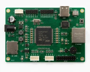
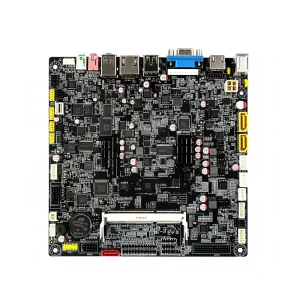
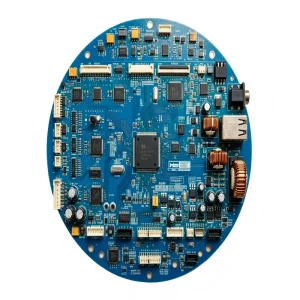
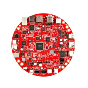
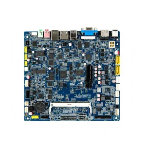
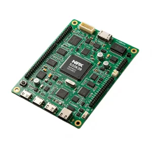
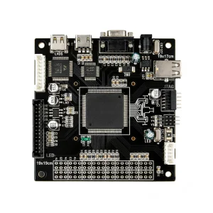
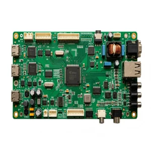
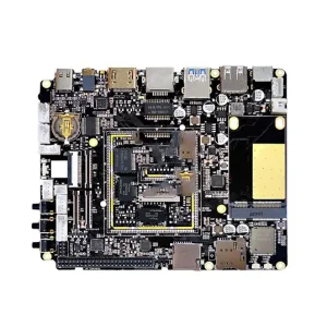
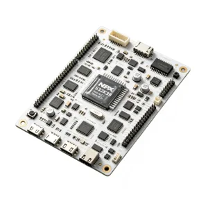
Review additional custom assemblies manufactured across our flexible SMT and automated box-build production lines.


Direct technical answers addressing production parameters, certifications, IP security, and component traceability.
Submit your design documentation to receive comprehensive DFM feedback, pricing analysis, and lead-time schedules within 24 hours.
