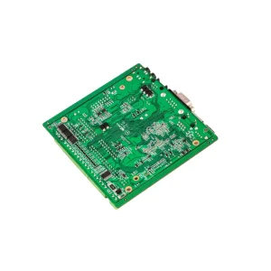
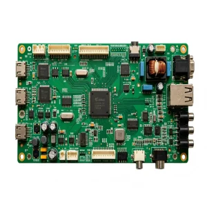
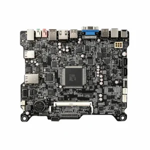
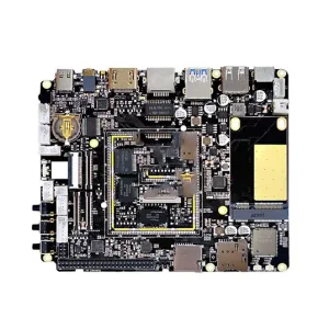
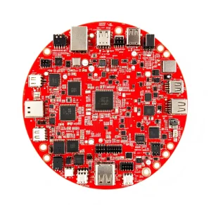
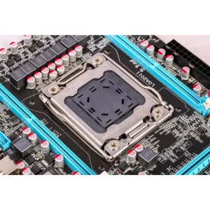
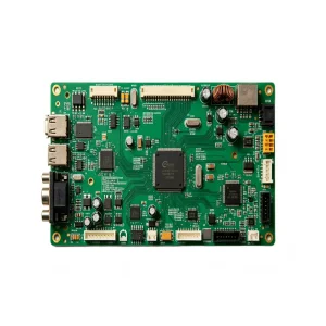
Proven manufacturing capability across optical high-speed communication, embedded sensing, industrial automation, and enterprise security platforms.
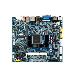

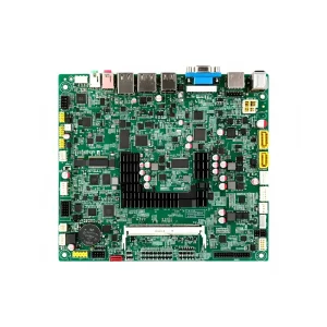
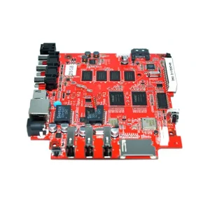
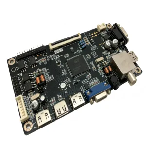
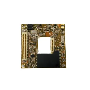
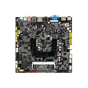
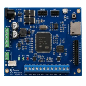
How intelligent automation, digital twins, and hyper-dense component assembly are redefining electronics contract manufacturing for mission-critical applications.
Equipped with ultra-high-speed modular placement heads capable of repeatable ±25µm accuracy at Cpk ≥ 1.33. Flawless handling of 01005 (0402 metric) and 03015 ultra-micro passive chips, fine-pitch quad-flat no-leads (QFN), and flip-chip ball grid arrays (BGA) down to 0.3mm pitch.
Over 65% of surface mount defects originate during stenciling. Our integrated 3D SPI platforms measure solder paste height, area, volume, and bridge coplanarity in real time. Feedback loops dynamically adjust squeegee pressure and automatic stencil wiping.
True 3D Automated Optical Inspection uses multi-angle moiré fringe projection to capture tombstoning, insufficient wetting, and co-planarity errors. Coupled with high-resolution off-axis 3D X-ray (AXI) for deep inspection of BGA solder ball voids (<10%), HIP, and micro-cracking.
Harnessing the Shenzhen & Greater Bay Area electronics super-cluster for rapid turnaround, component cross-referencing, and end-to-end MES digital traceability.
Within a 30-kilometer radius of our Bao'an facility lies the world's most concentrated ecosystem for multilayer PCB fabrication, silicon distributors, passive manufacturers, tooling fabricators, and custom CNC enclosure providers. This geographical advantage enables our engineers to source obsolete or hard-to-find active silicon, resolve component shortages within 24 hours, and drastically shorten NPI cycles.
Every single PCB entering our SMT line is laser-marked with a high-density 2D DataMatrix code. As the panel moves across solder paste printing, high-speed chip mounters, 10-zone nitrogen reflow ovens, and 3D optical inspection, our MES records machine parameters, feeder reel lot numbers, thermal profile curves, and inspection logs for 10-year forensic traceability.
Our team of 50+ senior hardware and industrial engineers performs comprehensive Design for Manufacturability (DFM) and Design for Testing (DFT) before launching physical pilot runs. By proactively identifying shadow effects in reflow, inadequate thermal relief pads, solder bridging risks, and single-source silicon vulnerabilities, we reduce engineering change orders (ECO) by up to 80%.
Certified execution complying with IATF 16949 automotive standards, ISO 13485 medical device systems, and IPC-A-610 Class 3 specifications.
Automotive grade PCBA requires zero-defect manufacturing, stringent Advanced Product Quality Planning (APQP), Production Part Approval Process (PPAP Level 3), and rigorous thermal cycling. We deliver ECU modules, Battery Management Systems (BMS), ADAS radar sensor boards, and in-vehicle infotainment assemblies that withstand harsh thermal vibration.
From pulse oximeters and patient monitors to blood gas analyzers and diagnostic imaging sub-assemblies, our medical lines operate under strict ISO 13485 protocols. Full device history records (DHR), bio-burden management, cleanroom conformal coating, and 100% boundary scan testing guarantee uncompromising patient safety.
Heavy-copper power inverters, high-speed optical transceivers, network firewalls, and smart grid meters operate in aggressive outdoor environments. We execute heavy selective wave soldering, robotic conformal coating (silicone, acrylic, polyurethane), automated potting, and functional environmental stress screening (ESS).
Comprehensive baseline specifications audited and sustained on our automated production lines in Shenzhen.
| Manufacturing Dimension | Standard Capability | Advanced / High-Density Capability | Verification & Test Protocol |
|---|---|---|---|
| SMT Passive Component Size | 0201 (0603 metric), 0402, 0603, 1206 | 01005 (0402 metric) & 03015 micro-passives | High-magnification 3D Optical Inspection |
| Fine Pitch IC & Micro-BGA | 0.40mm pitch QFP, SOP, BGA | 0.30mm pitch micro-BGA, CSP, POP, WLCSP | 3D Transmission X-ray with void calculation |
| Placement Accuracy & Repeatability | ±35 µm @ 3-sigma | ±25 µm @ Cpk ≥ 1.33 | Laser positioning & visual alignment cameras |
| PCB Dimensions & Geometry | 50mm x 50mm up to 510mm x 460mm | Max 1200mm x 500mm (Ultra-long LED / backplane) | Automatic conveyor width adjustment |
| PCB Layer Count & Core Substrates | 1 - 16 Layers (FR-4, CEM-3) | Up to 64 Layers (Any-layer HDI, Rogers, Ceramic, Polyimide Flex) | TDR impedance test & micro-sectioning |
| Reflow Environment & Thermal Zones | 8-Zone forced hot air convection | 10/12-Zone Reflow with Pure N2 Atmosphere (<500ppm O2) | ECD KIC real-time dynamic thermal profiling |
| Through-Hole Technology (THT) | Standard manual solder stations | Selective wave soldering in nitrogen tunnel + auto-insertion | IPC-A-610 Class 3 barrel fill >75% inspection |
| Testing & Quality Screening | Manual testing & basic ICT | Flying Probe, Bed-of-Nails ICT, Boundary Scan, Automated FCT | 100% functional test coverage with custom fixtures |
Transparent engagement frameworks tailored for international procurement teams, ensuring legal security, zero counterfeit ingress, and full environmental conformity.
We safeguard customer intellectual property with bilateral Non-Disclosure Agreements governed under internationally enforceable legal standards. Firmware code flashing occurs within secure, air-gapped programming suites equipped with encrypted server handshakes. Gerber files, schematics, and BOM architectures are segmented within enterprise role-based access controls.
Counterfeit components represent catastrophic liability in high-reliability applications. Our incoming quality inspection laboratory performs decapsulation, X-ray lead frame analysis, solderability testing, and silicon die marking verification against original component manufacturer (OCM) master databases prior to material reel stock storage in ESD moisture-barrier cabinets.
All solder alloys, fluxes, adhesives, conformal coatings, and assembled substrates strictly conform to EU RoHS Directive 2011/65/EU (and EU 2015/863 amendments) and REACH Regulation (EC No 1907/2006). Comprehensive material declarations (CMRT/EMRT) guarantee that all tantalum, tin, tungsten, and gold are responsibly sourced without conflict association.
Pioneering tomorrow's assembly thresholds: AI computer vision inspection, System-in-Package (SiP), photonics co-packaging, and autonomous AGV intralogistics.
Traditional rule-based AOI systems generate false call rates that burden secondary review teams. Our implementation of deep learning neural networks trains visual inspection models on millions of verified solder joints, drastically eliminating false rejects while flagging sub-surface anomalies, cold solder joints, and micro-voids with superhuman accuracy.
As electronic devices compress functionality into ultra-miniature form factors, planar surface mounting is converging with semiconductor packaging. Our roadmap integrates precision die placement, wire bonding, underfill dispensing, and substrate embedding to empower edge-AI sensor modules and ultra-compact wearable devices.
Full warehouse-to-line automation powered by automated guided vehicles (AGVs) delivers component reels and stencils to intelligent storage towers. Automated moisture-sensitive device (MSD) dry storage baking cycles coordinate seamlessly with line scheduling, eliminating human handling errors and atmospheric exposure risks.
Crucial insights for hardware engineers, global procurement executives, and commodity managers evaluating Chinese EMS manufacturing partners.
Expanding production horizons across high-voltage clean energy, biometric diagnostic sensors, electric mobility, and wireless communications.