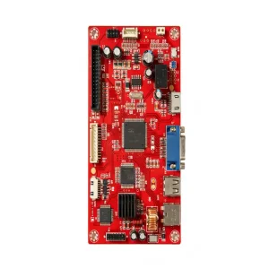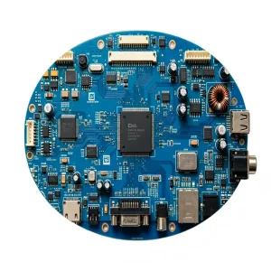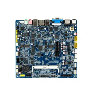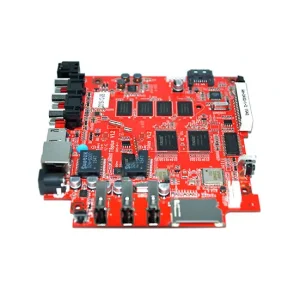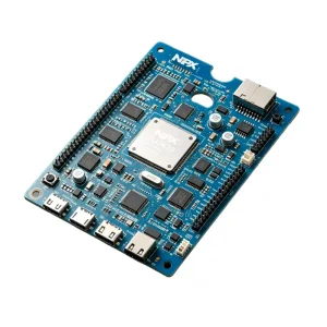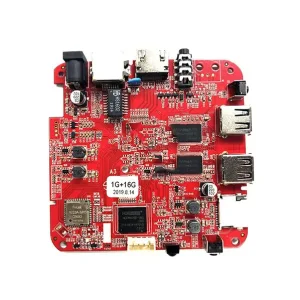
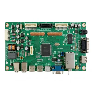
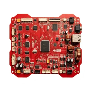
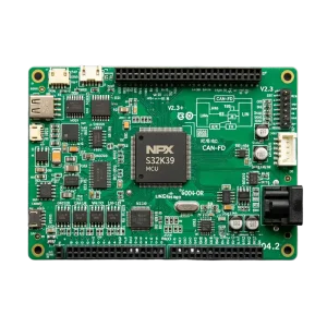
Featured turnkey sub-assemblies demonstrating high-density SMT mounting on rigid, flex, and complex dynamic substrates.
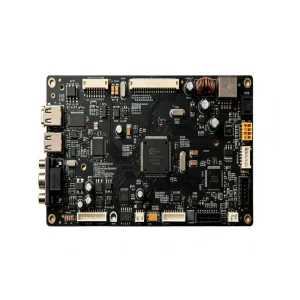
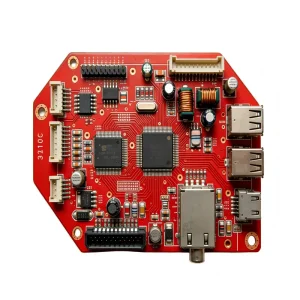
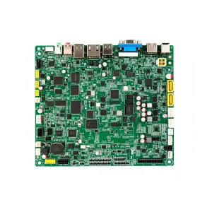
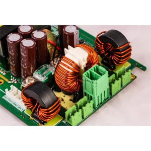
In modern electronic architecture, mechanical constraints dictate electrical form factors. Flexible printed circuits (FPCs) and rigid-flex systems have evolved from passive interconnects into primary spatial solutions.
Driven by miniaturization across medtech wearables, avionics, and high-performance computing, flexible circuits eliminate wire harnesses and multiple board-to-board connectors. This architecture reduces chassis volume by up to 65% and total package weight by 75% while mitigating human cabling assembly errors.
Continuous cyclic flexing applications—such as robotics articulation, camera gimbals, and foldables—demand engineered copper structures. Transitioning from standard Electro-Deposited (ED) copper to Rolled Annealed (RA) foils ensures over 10 million flex cycles without fatigue fracture or structural micro-cracking.
With 5G millimeter-wave and high-speed differential bus topologies operating beyond 28 Gbps, standard polyimide (PI) is augmented by Modified Polyimide (MPI) and Liquid Crystal Polymer (LCP). These substrates deliver low dielectric constants (εr ≈ 2.9 - 3.2) and dissipation factors (Df < 0.002) for signal integrity.
Evaluating China-based flexible circuit manufacturers requires analyzing end-to-end process control, supply-chain agility, and DFM expertise.
Global procurement teams face costly iterations when standard rigid PCB practices are misapplied to flexible circuits. Experienced tier-1 factories mitigate trace cracking through tear-drop routing, fillet enhancements, staggered via distribution, and selective stiffener placements (FR4, PI, stainless steel, and aluminum).
Component availability challenges require pre-qualified raw substrate networks. STHL maintains relationships with certified substrate manufacturers including DuPont Pyralux, Panasonic Felios, and Shengyi (SYTECH), ensuring flame retardancy (UL94 V-0) and compliance with IPC-4202, IPC-4203, and IPC-4204 specifications.
Mounting active ICs, fine-pitch BGAs (0.35mm pitch), and passive 01005 components onto flexible substrates requires advanced tooling. Turnkey lines utilize custom magnetic carriers, high-vacuum suction fixtures, and nitrogen-purged reflow ovens to prevent thermal warping or delamination.
Verified manufacturing envelope across STHL's cleanroom and SMT facilities in Bao'an, Shenzhen.
| Engineering Parameter | Standard Commercial Envelope | High-Precision / Advanced Matrix | Validation / Industry Benchmark |
|---|---|---|---|
| Layer Count Capability | 1 to 6 Layers (Pure FPC) / 2 to 12 Layers (Rigid-Flex) | Up to 10 Layers Flex / Up to 24 Layers Rigid-Flex | IPC-6013 Class 2 & Class 3 |
| Base Copper Type & Foil Thickness | 1/3 oz (12µm), 1/2 oz (18µm), 1 oz (35µm) ED/RA | 1/4 oz (9µm) Ultra-Thin, 2 oz Heavy RA Copper | IPC-4562 Rolled Annealed Copper Foil |
| Core Dielectric Substrates | Polyimide (PI) 12.5µm to 50µm Adhesive/Adhesiveless | Modified PI (MPI), Liquid Crystal Polymer (LCP) | IPC-4204 Adhesive/Adhesiveless Polyimide |
| Min. Trace Width / Clearance (W/S) | 0.050mm / 0.050mm (2 mil / 2 mil) | 0.035mm / 0.035mm (1.4 mil / 1.4 mil) via LDI | AOI Laser Direct Imaging Verification |
| Micro-Via Mechanical / Laser Drill | Mechanical: 0.15mm | Laser: 0.075mm (Blind/Buried) | Laser: 0.050mm UV/CO2 Dual-Head Processing | Cross-Section Microscopic Microsectioning |
| Coverlay & Surface Protection | Yellow / Black Polyimide Film (0.5 mil / 1.0 mil) | Photo-Imageable Flexible Solder Mask (LPI) | IPC-SM-840 Cross-Hatch Adhesion Test |
| Surface Finishes (Final Plating) | ENIG (Au: 1-3 μin, Ni: 120-240 μin), OSP, Immersion Tin | ENEPIG, Hard Gold Finger Plating (Au up to 30 μin) | X-Ray Fluorescence (XRF) Thickness Plating |
| Stiffener Integration | FR-4, Polyimide (PI), Stainless Steel 303/304 | Selective Aluminum Backers, Copper Heat Sinks | Automated Optical Alignment & Thermal Bonding |
| SMT Fine-Pitch Placement | 0201 passives, QFN, 0.4mm pitch CSP | 01005 chips, 0.3mm BGA pitch, Flip-Chip bonding | Full 3D Solder Paste Inspection (SPI) & 3D AOI |
Engineered flexible circuit solutions tailored to strict industry standards and environmental demands.
Medical instruments require high bio-compatibility and durability. Our assemblies serve in endoscopic probe linkages, wearable patient monitoring, and drug delivery systems. Manufactured in cleanroom environments with full lot-level trace validation for medical compliance.
Modern electric vehicles rely on FPCs to replace bulky battery harness wiring in Battery Management Systems (BMS). Our solutions resist prolonged thermal exposure (-40°C to +125°C), oil contamination, and shock, complying with PPAP Level 3 documentation requirements.
Avionics, flight navigation units, and Cockpit Voice Recorders (CVR) demand mechanical integrity under g-force shock and vacuum pressures. We deploy adhesiveless polyimides and rigid-flex designs that eliminate micro-voids, delivering performance under IPC-6013 Class 3 standards.
Defect prevention in flexible circuitry relies on strict environmental and process controls throughout fabrication and component assembly.
Polyimide films are susceptible to moisture absorption, which can cause micro-delamination during high-temperature lead-free reflow (260°C). STHL operates temperature-controlled, ESD-shielded workshops featuring automated moisture baking cycles and pre-SMT desiccator protocols.
Blind vias, micro-vias, and low-profile BGA solder connections undergo non-destructive high-resolution 3D X-Ray inspection. Regular metallurgical microsectioning verifies intermetallic compound (IMC) thickness, copper plating distribution, and absence of voiding in buried vias.
Our integrated Manufacturing Execution System (MES) links every production step—from raw laminate cutting to automated optical inspection (AOI) and final testing. Laser-etched QR identifiers provide part-level traceability matching ISO 9001 and automotive standards.
Continuous investment in advanced processes ensures support for emerging hardware architectures over the next decade.
Optimizing Vacuum Etching and high-precision Direct Imaging (LDI) to yield consistent 35µm trace/space configurations with uniform cross-sectional profiles across broad panel formats.
Deploying modified semi-additive techniques on ultra-thin seed layers, targeting sub-25µm trace geometries required for next-gen silicon packaging and fine-pitch AR/VR micro-displays.
Refining low-temperature thermoplastic bonding systems for multilayer Liquid Crystal Polymer structures to serve sub-terahertz applications and ultra-low insertion-loss radar.
Embedding bare silicon dies within flexible layers, eliminating wire bonds and external IC packaging to deliver ultra-compact form factors for edge computing and biomedical implants.
Key technical and supply-chain inquiries addressed by STHL's engineering directors.
Industrial, medical, and communication devices manufactured to international IPC standards.