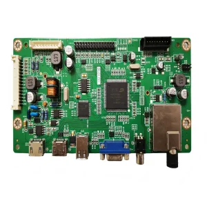
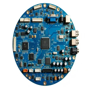
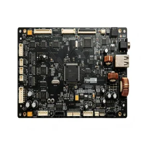
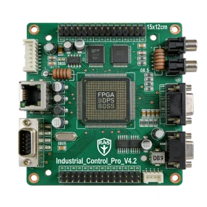
Explore our verified high-reliability production builds engineered for dynamic bend-cycles, automotive-grade harsh environments, and ultra-miniaturized electronic applications.
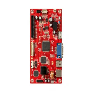
An authoritative analysis on polymer substrates, dynamic flexing fatigue, impedance matching, and high-yield turnkey EMS integration from China's premier electronic cluster.
In modern electronic hardware architectures, Flexible Printed Circuits (FPC) and Rigid-Flex PCBs have evolved from simple spatial interconnects into core architectural components. With the rapid convergence of high-density edge AI computing, advanced electric vehicle battery management architectures (EV BMS), implantable medical telemetry, and aerospace inertial guidance, mechanical enclosure boundaries have shrunk while signal integrity requirements have skyrocketed. As a pioneer in turnkey electronic manufacturing based in Bao'an, Shenzhen since 2006, STHL delivers full-lifecycle flex circuit solutions conforming to rigorous IPC-6013 Class 3, IATF 16949, and ISO 13485 standards.
The manufacturing superiority of flexible circuits hinges on base substrate material science. Traditional rigid PCBs rely heavily on woven glass-reinforced epoxy (FR-4), which presents mechanical rigidity, high dielectric losses at microwave frequencies, and vulnerability to continuous vibrational strain. In contrast, precision flex circuit fabrication uses polyimide (PI) film or next-generation Liquid Crystal Polymer (LCP) cores, providing exceptional dielectric constants (Dk of 3.2 to 3.4 for PI; 2.9 for LCP) and dissipation factors (Df down to 0.002). By utilizing adhesiveless copper clad laminates (FCCL) with electro-deposited (ED) or rolled annealed (RA) copper foil, our facility enables dynamic bending fatigue thresholds exceeding 500,000 continuous flexure cycles at a bend radius tighter than 6x board thickness.
Direct cast-on-copper polyimide architectures eliminate thermally unstable acrylic or epoxy adhesives. This yields superior thermal dissipation, tighter micro-via drill geometries, and outstanding reflow survival under lead-free conditions up to 260°C peak temperatures.
Combining advanced Laser Direct Imaging (LDI) with non-contact vacuum semi-additive processing (mSAP) enables minimum line width and line spacing (L/S) down to 35μm / 35μm. This permits dense BGA escape routing under 0.35mm pitch micro-controllers.
Precision cross-hatch ground planes, coplanar waveguide routing, and controlled coverlay dielectric thickness guarantee single-ended (50Ω ± 7%) and differential (90Ω/100Ω ± 8%) high-speed transmission lines up to 28 Gbps per lane without signal reflection.
Navigating complex dynamic mechanical constraints across the automotive electrification, high-density avionics, intelligent healthcare, and consumer edge compute sectors.
The global electronic hardware manufacturing industry is experiencing an unprecedented structural pivot away from bulky wiring harnesses, mechanical crimp terminals, and modular connector blocks. In Tier-1 automotive and industrial automation ecosystems, physical cabling represents the third heaviest sub-assembly and a primary vector of field failure due to thermal expansion, localized vibration, and manual assembly tolerances. China Flex Circuit PCB manufacturing services have directly resolved this bottleneck by engineering monolithic flexible busbars, multilayer flex-harness replacements, and hybrid rigid-flex motherboards.
In electric vehicle battery packs, high-voltage battery management systems (BMS) have systematically shifted from traditional NTC thermistor wire harnesses to integrated FPC sensing ribbons. Our automotive-qualified flex boards integrate cell voltage tap-off fingers, temperature sensors, and fuse protection within a single 0.25mm thin laminated polyimide strip. Under our certified IATF 16949 line control, assemblies endure continuous vibrational shock tests up to 30G and thermal cyclings ranging between -40°C and +125°C, providing fail-safe operation for over 15 years.
Medical devices demand absolute biocompatibility, miniaturization, and micro-motion durability. From flexible multi-electrode arrays in ECG monitors to steerable endoscopy camera snakes, STHL manufactures flexible PCB assemblies using medical-grade coverlays and immersion pure gold (ENIG) or Electroless Nickel Electroless Palladium Immersion Gold (ENEPIG) finishes. Compliant with ISO 13485, every batch undergoes automated optical inspection (AOI) and plasma surface treatment to guarantee void-free micro-underfill around sensitive bio-sensor chips.
Overcoming flex substrate warpage, thermal lamination distortion, and micro-component coplanarity during turnkey surface mount assembly.
Surface mount assembly (SMT) on flexible circuits represents one of the most intricate challenges in electronic manufacturing services (EMS). Unlike rigid FR-4 substrates that maintain planarity under convective heat, polyimide is hygroscopic (absorbing up to 1.5% moisture by weight) and mechanically elastic. Subjecting an unstabilized FPC to a lead-free reflow profile reaching 245°C–255°C will provoke instantaneous outgassing, blister formation, copper delamination, and severe spatial shrinkage.
At STHL, our engineering methodology neutralizes these physical phenomena via systematic pre-baking cycles (120°C for 4 hours in nitrogen-purged ovens), custom high-precision magnetic vacuum carrier pallets, and real-time 3D Solder Paste Inspection (SPI). Our high-speed Fuji and Panasonic SMT lines routinely mount 01005 passive chips, 0.3mm pitch WLCSP silicon, and high-pin-count micro-BGAs with 15μm placement accuracy.
| Critical Engineering Parameter | Standard Flex Production Capability | Advanced Aerospace / Medical Tier | Quality Verification Protocol |
|---|---|---|---|
| Layer Count Capability | 1 - 6 Layers (Single, Double, Multi-layer Flex) | Up to 16 Layers (Rigid-Flex Multilayer Stackup) | Cross-Section Microscopic Analysis |
| Min. Line Width / Line Spacing (L/S) | 50μm / 50μm (2 mil / 2 mil) | 35μm / 35μm (1.4 mil / 1.4 mil via mSAP) | Automated Optical Inspection (AOI) |
| Laser Blind & Buried Microvia Diameter | 75μm (0.003 inch) | 50μm (UV Laser Trepanning) | X-Ray Tomography & Scanning SEM |
| Polyimide Base Dielectric Thickness | 25μm (1.0 mil) / 50μm (2.0 mil) | 12.5μm (0.5 mil) Ultra-Thin Polyimide | Laser Micrometry & Beta-Backscatter |
| Surface Finish Metallization | Lead-Free HASL, ENIG (Ni: 3-5μm, Au: 0.05-0.1μm) | ENEPIG, Immersion Silver, Soft Bondable Gold | XRF Spectrometry Coating Thickness |
| Stiffener Integration Options | FR-4, Stainless Steel 304, Aluminum Alloy | Polyimide Stiffeners, Ceramic Heatspreaders | Peel Strength Adhesion Testing (ASTM D1876) |
| Impedance Tolerance Control | ± 10% Standard Control | ± 7% Tightened High-Frequency Control | 100% TDR (Time Domain Reflectometry) |
Safeguarding western intellectual assets while providing transparent supply chain provenance and rapid bilingual engineering collaboration.
For international procurement directors, Chief Technology Officers, and supply chain executives in North America, Europe, Japan, and Oceania, qualifying an offshore manufacturing partner extends beyond pure fabrication pricing. Key operational risks include intellectual property leaks, sudden component obsolescence, regulatory export non-compliance, and cross-border engineering miscommunications. STHL’s institutional infrastructure has been engineered specifically to mitigate these enterprise friction points.
Every engineering transaction is governed by enforceable bilateral non-disclosure agreements before Gerber transmission. Data pipelines are encrypted under enterprise AES-256 protocols, with physical server access segregated across secure internal subnets to safeguard confidential ASIC designs and proprietary firmware assets.
Leveraging direct relationships with 100+ authorized electronic component distributors (including Arrow, Avnet, Digi-Key, Mouser, Microchip, and STMicroelectronics), we guarantee 100% factory-original silicon. Anti-counterfeiting incoming inspection includes decapsulation, lead-frame spectrometry, and lot date-code verification.
Our turnkey flex assemblies fully comply with international environmental mandates, including EU RoHS 3 Directive (2015/863/EU), REACH (EC 1907/2006), and halogen-free restrictions (IEC 61249-2-21). Outgoing packages feature vacuum moisture barrier bags (MBB) with active desiccant and HIC indicator cards meeting JEDEC J-STD-033C.
Review how STHL's integrated flex design-for-manufacturability (DFM) interventions unlocked reliability milestones in demanding field conditions.
Challenge: An energy instrumentation client experienced repeated trace cracking in subterranean MWD (Measurement While Drilling) sensors exposed to 175°C downhole heat and intense multi-axis harmonic vibration.
Solution: We implemented an adhesiveless 4-layer rigid-flex assembly using high-Tg polyimide, curved trace topology with filleted teardrop pads, and bonded aluminum backing stiffeners. Trace fracturing was completely eradicated in validation runs exceeding 1,200 operating hours.
Challenge: High-frequency impedance mismatches and micro-crack failures occurred across the tight hinge flex zone (radius < 1.5mm) in a handheld dual-screen industrial computer.
Solution: STHL utilized rolled-annealed 1/3 oz copper with neutral-axis layer balancing. The outer dielectric coverlay was laser-skived in the flex window, and a silver EMI conductive film was deployed for shield continuity, achieving 600,000 flawless dynamic cycles.
Challenge: Severe weight budgets and tight volume limits prevented traditional enclosure wiring between gyro-sensor boards and the main flight guidance processor.
Solution: A monolithic 8-layer rigid-flex circuit was engineered, integrating 4 rigid FR-4 component zones bridged by 2 internal polyimide dynamic flex arms. Weight decreased by 64%, manual harness assembly time was eliminated, and high-G launch survival was verified under MIL-STD-810H.
Pioneering future-ready materials and manufacturing processes for sub-millimeter edge computing, 5G/6G millimeter wave flex, and ultra-high-density interconnects.
The boundary between traditional semiconductor packaging and printed circuit board manufacturing is rapidly dissolving. As monolithic systems-on-chip (SoCs) transition into modular chiplet architectures and millimeter-wave communication bands expand past 60 GHz, flexible circuitry is moving toward sub-20μm geometries and specialized low-loss fluoropolymer matrices.
While polyimide remains the industrial workhorse, its dielectric loss factor (Df ~0.008 at 10 GHz) introduces intolerable insertion loss at high millimeter-wave radar and satellite communication bands. Our R&D facility has industrialized true thermoplastic LCP processing, exhibiting a Dk of 2.9 and Df of 0.002 up to 110 GHz, paired with near-zero moisture absorption (<0.04%).
To break through physical 2.5D packaging limitations, STHL is pioneering embedded passive component technology (EPCT) inside flexible polyimide inner cores. Thin-film planar resistors and high-permittivity ceramic capacitors are embedded directly into internal layers, liberating up to 45% of surface real estate for core active micro-controllers.
Transitioning from subtractive chemical acid etching toward closed-loop additive Roll-to-Roll (R2R) photolithography reduces water consumption by 70% and copper waste by 85%. This advanced method enables endless-run flexible cables for large EV battery architectures while supporting global carbon neutrality mandates.
Clear, technically rigorous answers for hardware engineering leads and global electronics sourcing managers.
Engineered for harsh operating parameters, advanced telecommunications, radar sensors, and mission-critical consumer electronics.
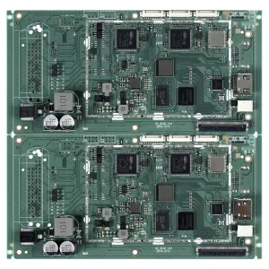
Whether you need 5 prototype boards for proof-of-concept testing or 500,000 production units under an automated MES environment, our engineering team in Shenzhen is ready to review your project with zero obligation.