Explore our integrated printed circuit board assembly executions across intelligent IoT, medical diagnostics, vision control, and connected infrastructure.
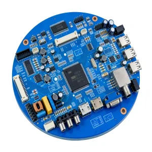
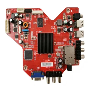
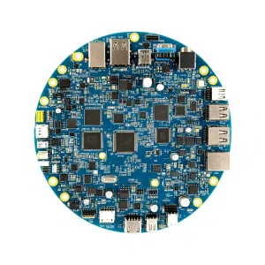
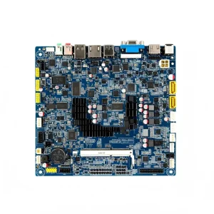

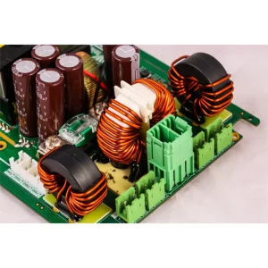
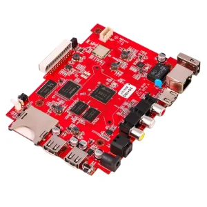
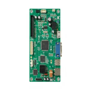
In modern electronic hardware product realization, procurement fragmentation represents the greatest single operational vulnerability for original equipment manufacturers (OEMs).
Dividing bare PCB fabrication, passive and active semiconductor procurement, and surface-mount technology (SMT) across disconnected tier vendors introduces critical overhead. Inconsistencies in fabrication tolerances, moisture sensitivity handling (MSD), and logistics handoffs elevate Total Cost of Ownership (TCO) and obscure fault accountability during qualification.
Situated in Shenzhen—the epicentre of global electronic innovation—Shenzhen STHL Electronics Co., Ltd. (founded in 2006) operates an advanced 10,000+ m² smart facility. Operating 7 automated high-speed SMT lines, 2 dual-wave DIP soldering lines, 2 precision functional test lines, and 2 box-build lines, our facility converts complex BOMs into market-ready boxed hardware.
Every turnkey production run is managed under closed-loop ERP and MES governance. We guarantee full component traceability, automated DFM/DFA engineering audits, zero Minimum Order Quantity (no MOQ) barriers, a sustained 99.5% on-time delivery rate, and an exceptional 99.0% qualified first-pass shipment yield across North America, Europe, and Asia.
Turnkey assembly in China has transitioned from cost-arbitrage commoditization to certified, high-mix, high-complexity systems engineered to withstand severe environments.
Governed by strict IATF 16949 automotive procedures, we manufacture heads-up displays (HUD), engine control units (ECU), battery management systems (BMS), and smart automotive lighting. Solutions undergo thermal shock cycling (-40°C to +125°C), high-vibration stress testing, and automated conformal coating to prevent electrochemical migration under harsh under-hood environments.
Certified under ISO 13485, our medical PCBA workflow supports clinical-grade blood pressure monitors, physiological recorders, micro-sensor implants, and diagnostic monitors. We deliver 100% component traceability, zero-flux residue cleaning protocols, and biological compatibility assurance with stringent risk mitigation matrices conforming to ISO 14971.
Precision computing units such as Air Data Computers (ADC) and GNSS positioning modules demand ultra-dense impedance control, differential pair routing, and high-frequency Rogers/PTFE hybrid substrate integration. Assemblies comply with IPC-A-610 Class 3 avionics standards, employing automated X-ray inspection (AXI) for BGA solder voiding below 15%.
Handling high current densities, transient surge suppression, and thermal dissipation challenges in high-power solar inverters and automated factory PLC controllers. Incorporates thick-copper circuitry (up to 4oz-6oz), ceramic substrates, and custom wire harness potting to ensure continuous 24/7/365 uninterrupted industrial runtimes.
Compact, battery-operated IoT sensors, wireless mesh routers, and secure access points require microscopic component placement down to 01005 passives and 0.35mm pitch fine-pitch QFNs. Complete RF testing, antenna tuning, and custom enclosure sonic welding ensure optimal signal integrity and IP68 environmental hermeticity.
From industrial high-brightness human-machine interfaces (HMI) to lightweight consumer and commercial tablets, our lines execute high-yield micro-BGA assembly, optical bonding, integrated ribbon-cable interfacing, and automated multi-touch display functional testing.
A transparent breakdown of production capabilities, machine limits, and IPC-standard quality controls verified across our Shenzhen SMT lines.
| Manufacturing Dimension | Technical Capability Limit | Standard Operating Tolerance | Process Validation Standard |
|---|---|---|---|
| Assembly Methods | SMT, Through-Hole (THT/DIP), Mixed Assembly, Double-Sided SMT | Coplanarity < 0.08mm | IPC-A-610 Class 2 / Class 3 |
| Min. Component Placement | 01005 (0402 metric) chips, 0.3mm pitch Micro-BGA, QFN, CSP | Placement accuracy ±0.025mm | 3D Solder Paste Inspection (SPI) |
| Max. PCB Dimensions | 610mm × 1200mm (Ultra-long LED & Backplane Capability) | Board thickness 0.2mm to 6.0mm | Automated Optical Inspection (AOI) |
| Substrate Technology | FR-4 (High-Tg), Rogers, Aluminum, Rigid-Flex, Polyimide, Ceramic | Impedance control ±5% to ±10% | Micro-section & TDR Analysis |
| Soldering Capabilities | 10-Zone Reflow (Nitrogen Purge), Lead-Free SAC305, Selective Wave | Profile tracking within ±1.5°C | Real-time KIC Thermal Profilers |
| Advanced Inspection | 3D AOI (Koh Young), Inline Real-time 3D X-Ray (AXI), First Article Test | Voiding analysis < 15% on BGA balls | J-STD-001 Verification |
| Value-Added Testing | In-Circuit Testing (ICT), Flying Probe, Custom Functional Testing (FCT) | Firmware programming & MAC ID inject | 100% Test Vector Pass Metric |
| Protective Finishing | Automated Conformal Coating (Acrylic, Polyurethane, Silicone), Potting | Thickness 25µm - 75µm uniform | UV Inspection & Salt Spray Test |
Procuring microchips and specialized passives amidst global supply chain swings requires direct factory relationships, counterfeit mitigation, and predictive obsolescence management.
STHL maintains direct strategic manufacturer accounts and authorized distribution channel linkages with 100+ premier distributors worldwide, including Digi-Key, Mouser, Arrow Electronics, Avnet, Farnell, and Future Electronics. Our localized procurement network across China enables immediate access to original factory inventory from STMicroelectronics, Microchip, Texas Instruments, TDK, and Littelfuse.
Counterfeit electronic components present massive operational risks to high-reliability applications. STHL operates an inbound incoming quality control (IQC) laboratory equipped for decapsulation testing, X-ray leadframe inspection, solderability testing, and microscopic surface markings verification, ensuring zero substandard or refurbished parts ever hit production feeders.
When long lead times (e.g., 52+ weeks) threaten production schedules, our 50+ engineering team executes immediate Form-Fit-Function (FFF) BOM scrubbing. We cross-reference high-performing domestic alternatives or alternate tier-1 footprints to maintain identical electrical parameters, thermal tolerances, and pinouts—compressing production lead times from months down to weeks while yielding 15% to 30% BOM cost reduction.
A deterministic, ISO-compliant manufacturing trajectory governed by MES data logging ensures complete real-time visibility across every phase of your turnkey hardware journey.
Bilateral NDA sign-off followed by full review of Gerber, centroid, and BOM files to resolve thermal traps, solder bridging, and trace clearance conflicts within 24 hours.
Parts pulled from approved franchise distributors and bare boards fabricated to exact impedance, copper weight, and soldermask specifications.
High-precision laser stencil application with automated 3D Solder Paste Inspection (SPI) verifying paste volume, height, alignment, and area.
Multi-axis Yamaha and Panasonic pick-and-place systems rapidly mount passives down to 01005, fine-pitch BGA, and complex ICs with optical verification.
10-zone multi-profile reflow under a nitrogen inert atmosphere, eliminating oxidation, preventing tombstoning, and ensuring perfect intermetallic bond formation.
Koh Young 3D AOI checks component offsets, solder fillets, and polarity, followed by inline X-Ray (AXI) analyzing internal ball array connections beneath BGAs.
Custom bed-of-nails or flying probe testing verifies passive circuits, executes IC bootloader flash, and cycles inputs/outputs under simulated operational conditions.
Conformal coating, mechanical chassis assembly, wire harness integration, ESD anti-static vacuum packaging, and air/ocean dispatch to 90+ global destinations.
Operating under world-class regulatory oversight, STHL safeguards customer intellectual property, guarantees environmental sustainability, and assures full customs border compliance.
Western hardware designers frequently cite IP protection as their primary hesitation with overseas manufacturing. STHL enforces enforceable non-disclosure agreements (NDAs) prior to file intake. Gerber files, BOM registries, and proprietary firmware are sequestered on isolated, encrypted internal servers accessible solely by authorized project lead engineers.
Our operational systems are fully certified under four cornerstone international benchmarks: ISO 9001:2015 (Quality Management Systems), IATF 16949:2016 (Automotive Defect Prevention), ISO 13485:2016 (Medical Device Traceability), and ISO 14001:2015 (Environmental Stewardship), ensuring audit compliance across high-scrutiny industries.
All turnkey assemblies strictly comply with RoHS 3 (EU Directive 2015/863), eliminating hazardous substances such as Lead, Mercury, and Cadmium. Products adhere to REACH (EC 1907/2006) chemical safety mandates, carry CE/FCC testing documentation, and utilize UL94V-0 flammability-certified laminates ready for customs clearance.
Continuous investment into automated intelligence and advanced packaging technologies positions STHL at the leading edge of modern electronics assembly.
Integrating deep learning computer vision algorithms into our inline 3D AOI inspection stations drastically reduces false calls while elevating defect escape containment to near-zero PPM levels. The neural network accurately classifies micro-bridging, tombstoning, and insufficient wetting down to microscopic thresholds.
As wearable electronics, edge IoT nodes, and high-performance computing hardware shrink, STHL continues to expand advanced Any-Layer HDI (up to 12+ layers), laser micro-via drilling (down to 0.075mm), fine line width/spacing (2.5/2.5 mil), and stacked micro-vias for cutting-edge computing boards.
We are actively building real-time MES data portals that allow overseas procurement and hardware engineering directors in the US and Europe to view real-time assembly line parameters, SPI solder height profiles, and reflow thermal curves directly through secure cloud dashboard APIs.
Clear, definitive answers to technical, commercial, and logistical questions asked by overseas engineering teams before committing files to production.
In consigned assembly, you source, kit, and dispatch every electronic component and bare PCB to our Shenzhen facility, assuming all shipping delays, tariff complexities, and scrap buffer risks. In Full Turnkey assembly, STHL manages everything: bare PCB fabrication, component procurement via authorized channels, engineering DFM verification, SMT/THT assembly, testing, and final packaging under a single consolidated invoice and guaranteed schedule.
STHL has no minimum order quantity (No MOQ). We readily build 5-piece functional prototype engineering runs using the exact same automated pick-and-place lines, solder paste stencils, and reflow ovens as our high-volume multi-thousand production runs. This guarantees seamless transitions from prototype validation directly into volume production without line-transfer recalculation.
We enforce a strict zero-counterfeit procurement charter. All semiconductors and passive parts are procured exclusively from original chip fabricators or franchised global distributors (Digi-Key, Mouser, Arrow, Avnet, Farnell). Incoming lots undergo rigorous incoming IQC inspection using X-ray verification, high-magnification digital microscopy for re-topping analysis, and solderability tests matching IDEA-STD-1010B standards.
To deliver an official, line-item quotation within 24–48 hours, our engineering staff requires: (1) Gerber RS-274X or ODB++ files, (2) Bill of Materials (BOM) in Excel with manufacturer part numbers (MPN), descriptions, and quantities, (3) Pick-and-Place Centroid file (X, Y coordinates and component rotation), and (4) Test Specifications or mechanical box-build assembly drawings if box-build is requested.
Fine-pitch Ball Grid Arrays (BGAs), Quad Flat No-leads (QFNs), and land grid array packages conceal their solder joints underneath the chip body, preventing optical inspection. STHL verifies 100% of these joints using inline transmission 3D X-Ray Inspection (AXI). We calculate exact solder void percentages against IPC-A-610 Class 3 limits (mandating solder voiding remain below 15% to guarantee thermal and mechanical reliability).
Yes. Beyond surface-mount and through-hole soldering, we operate two dedicated functional test (FCT) lines. We load customer-provided hex/bin firmware onto microcontrollers, program EEPROMs, verify radio frequency RF transmit/receive strengths, validate sensor inputs, and run customized burn-in stress cycles. Pass-fail serialization logs are archived directly within our MES database for total batch traceability.
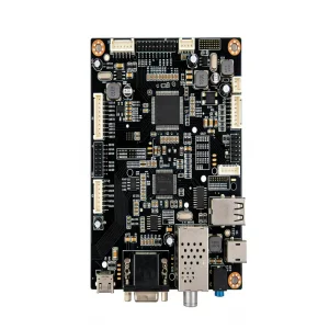
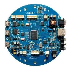
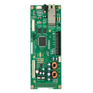
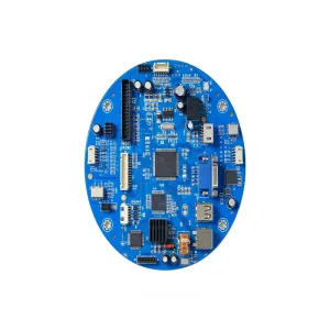
Explore our advanced manufacturing executions across environmental telemetry, high-power renewable conversion, aviation computing, and spatial positioning.
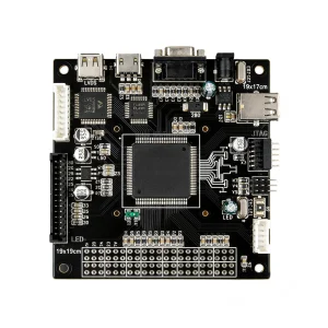


Directly upload your Gerber, BOM, and assembly schematics. Our Shenzhen engineering team will execute a complete DFM/DFA feasibility analysis, verify sourcing pipelines, and deliver an official line-item quotation within 24 hours.
Request DFM Audit & Turnkey Quote