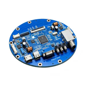
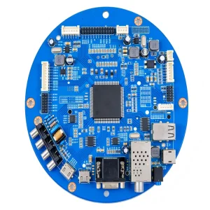
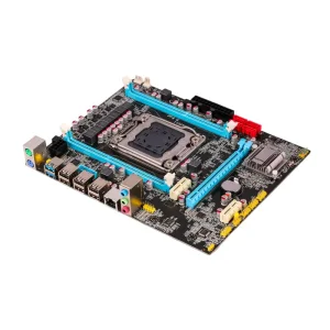
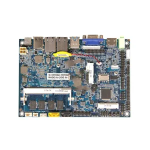
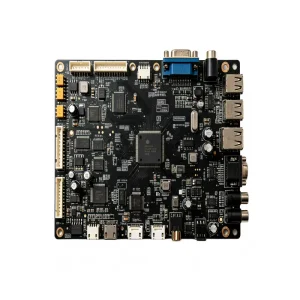
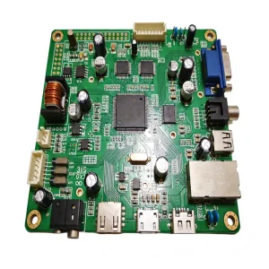
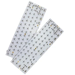
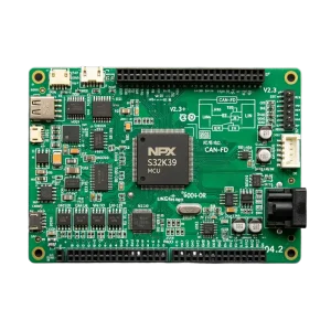
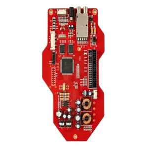
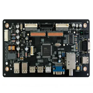
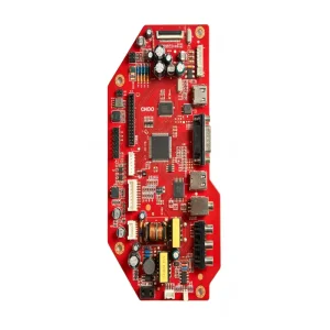
Explore production-verified assemblies engineered across specialized medical, industrial, commercial, and energy sectors. Every unit reflects our rigorous engineering design reviews, precision component mounting, and multi-tier functional testing.
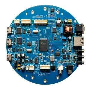


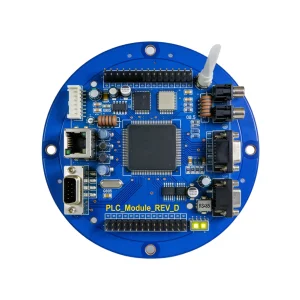
Industrial original equipment manufacturers (OEMs) and cutting-edge hardware enterprises are systematically abandoning fragmented fabrication models in favor of unified, full turnkey electronics manufacturing.
Historically, procurement directors bifurcated product manufacturing into three disjointed silos: purchasing bare PCBs from a board fabricator, sourcing active and passive silicon components via regional brokers, and assigning assembly to an SMT subcontractor. This dispersed approach introduces compounded lead times, disputed RMA liability, and catastrophic inventory dead-stock.
Full Turnkey PCB Assembly unifies raw circuit board fabrication, precision component procurement, surface-mount placement, through-hole insertion, in-circuit validation, and end-of-line enclosure assembly under a single contract manufacturer with absolute traceability.
Modern bill of materials (BOM) complexity frequently exceeds 400 unique line items per board. When unexpected obsolescence, allocation shortages, or rolling engineering change orders (ECO) occur, a segmented vendor model inevitably descends into cross-vendor finger-pointing regarding soldering wettability, pad oxidation, or moisture sensitivity level (MSL) handling.
Turnkey partners assume unilateral fiscal and technical responsibility. Our engineers execute proactive component life-cycle scrubs, recommend footprint-compatible alternates, and ensure board stack-ups strictly conform to fabricator DFM rules before raw copper is etched.
The acceleration of IoT deployment, industrial robotics, electric vehicle charging infrastructure, and customized medical diagnostic hardware requires extreme manufacturing agility. Hardware start-ups and enterprise R&D groups cannot sustain 16-week traditional ramp times.
Agile turnkey manufacturing shortens product introduction cycles from months to days. Rapid NPI (New Product Introduction) workflows validate mechanical fits, RF matching networks, and solder profiles concurrently with prototype pilot batches, achieving high first-pass yields.
Shenzhen, China represents the world's most concentrated microelectronics engineering cluster. Operating inside this epicenter gives our clients unparalleled speed, cost-efficiency, and resilience.
Our 10,000+ m² facility located in Bao'an District, Shenzhen, operates within minutes of Asia’s largest component distribution channels and primary silicon manufacturer hubs. Over 100 authorized Tier-1 component agents and regional authorized suppliers provide direct inventory access to 500,000+ verified part numbers.
When engineering BOMs encounter unexpected factory allocations or abrupt semiconductor line stoppages, our localized procurement team inspects and obtains authentic factory-sealed reels within 4 hours, compared to weeks for Western counterparts.
Bare board fabrication in the Guangdong-Hong Kong-Macao Greater Bay Area benefits from mature copper laminate infrastructure (FR-4, Rogers, Megtron 6, Polyimide, and Aluminum substrates). Sub-tier processes—such as ENIG, ENEPIG, Immersion Silver, laser micro-via drilling, and blind/buried via filling—are completed rapidly without cross-border transport.
Quick-turn prototypes move from Gerber CAM layout extraction to fully assembled, X-ray-verified PCBA samples in as little as 48 to 72 hours.
Turnkey assembly in Shenzhen extends well past SMT board placement. It integrates tooling, plastic injection molding, CNC precision milling, custom wire harnesses, silicone gaskets, and die-cut shielding within an integrated supply ring.
We configure complete box-build operations—mounting the PCBA into bespoke aluminum or ABS enclosures, routing internal coaxial and power harnesses, applying UV-curable conformal coatings, and loading end-user retail packaging ready for worldwide dropshipping.
A multi-stage quality assurance system built around real-time MES traceability, DFM verification, and rigorous defect prevention.
Prior to cutting copper or ordering parts, our senior CAM engineering team reviews your Gerber RS-274X/ODB++, BOM, schematic, and IPC centroid files. We evaluate pad-to-trace clearances, solder mask dam integrity, thermal relief configurations, and automated test point coverage.
Design for Manufacturability (DFM), Assembly (DFA), and Test (DFT) checks eliminate tombstoning risks, BGA bridging tendencies, and thermal mass shadowing during reflow soldering.
Counterfeit semiconductor suppression requires strict protocol. All incoming components are managed through dry-cabinet storage and ESD-controlled warehouses. Lot numbers, reel date-codes, and moisture barrier bag (MBB) desiccant states are digitally recorded in our ERP system.
IQC conducts decapsulation audits, pin-oxidation microscopy, solderability testing, and XRF material composition verification to guarantee 100% genuine components before production release.
Production runs on high-precision Yamaha and Panasonic SMT lines. DEK automatic stencil printers with 2.5D solder paste inspection (SPI) verify paste height, volume, and alignment offset before component placement.
Dual-beam modular placers handle passive chips down to 01005 (0402 metric) and micro-BGAs down to 0.3mm ball pitch, maintaining tight placement tolerances at high speeds.
Our 10-zone convection reflow ovens run tailored 9-point thermal profiling calibrated via KIC thermal profilers for SAC306, SnBi, and low-temperature lead-free solder alloys. Through-hole components undergo selective soldering or nitrogen-inerted wave soldering to prevent joint oxidation.
Optimal wetting angles, complete intermetallic compound (IMC) boundary formation, and clean solder fillets adhere to IPC-A-610 Class 3 workmanship standards.
Every single board passes automated inline 3D AOI to check for component presence, polarity orientation, skew, solder bridging, and insufficient wetting. Hidden solder joints—such as BGAs, QFNs, bottom-terminated components (BTC), and LGA pads—undergo 3D X-ray inspection (AXI).
AXI validates solder voiding thresholds well below the 15% threshold, preventing premature field failures from thermal hot-spots or mechanical fatigue.
Assemblies undergo Flying Probe or customized In-Circuit Testing (ICT) bed-of-nails checks to verify net resistance, capacitance, and diode polarity. Custom functional test jigs flash target bootloaders and execute deep communication protocol tests (CAN, RS-485, BLE, Wi-Fi, Ethernet).
Automated robotic spray systems apply silicone, acrylic, or polyurethane conformal coatings for harsh environment sealing. Assemblies are then integrated into enclosures, labeled with serialized laser barcodes, and boxed for global dispatch.
A side-by-side technical reference outlining our production parameters, equipment thresholds, and processing limits.
| Technical Domain | Standard Production Capability | Advanced / High-Precision Threshold |
|---|---|---|
| Assembly Types & Technology | Surface Mount (SMT), Through-Hole (THT/DIP), Mixed SMT/THT, Single & Double-Sided Placement | PoP (Package on Package), Press-fit, Chip-on-Board (COB), Micro-BGA, Fine-Pitch QFP |
| SMT Component Range | 0201 chip, 0402, 0603, 0805, 1206 passives, SOIC, TSSOP, QFP down to 0.4mm pitch | 01005 (0402 metric) passives, 0.3mm Ultra-Fine BGA, CSP, WLCSP, LGA, BGA up to 75x75mm |
| PCB Substrate Diversity | Standard FR-4 (Tg 130–150°C), High-Tg FR-4 (Tg > 170°C), Aluminum metal-core (1-3 W/m-K) | Polyimide Flex, Rigid-Flex (up to 16L), Rogers, Ceramic (Al2O3/AlN), Heavy Copper (up to 12oz) |
| Board Geometry & Layer Count | 2 to 16 Layers; Min dimensions: 50 x 50mm; Max dimensions: 460 x 610mm | 1 to 48 Layers; 1-4 Step HDI (Any-Layer Via); Max panel dimension: 600 x 1200mm |
| Board Thickness & Tolerances | 0.4mm to 3.2mm ±10%; Min drill hole: 0.2mm; Aspect Ratio 8:1 | 0.15mm to 6.0mm ±8%; Laser via: 0.075mm; Aspect Ratio 12:1; Controlled Impedance ±5% |
| Surface Finishes | Lead-Free HASL, OSP, Electroless Nickel Immersion Gold (ENIG 1–3u" Au) | ENEPIG, Immersion Tin, Immersion Silver, Hard Gold Plating (Finger gold up to 30u") |
| Automated Inspection & Testing | Inline 2D/2.5D SPI, Offline/Inline 3D AOI, In-Circuit Test (ICT), Manual Visual QC | High-Res 3D Inline AXI (X-Ray), Flying Probe Test, Custom Functional Test Jigs, Boundary Scan |
| Quality Standards & Credentials | IPC-A-610 Class 2 Workmanship, ISO 9001:2015, ISO 14001:2015 | IPC-A-610 Class 3 High Reliability, IATF 16949 (Automotive), ISO 13485 (Medical Devices) |
| Traceability & Digital Control | Standard batch-level tracking, manual traveler route cards, BOM revisions | Real-time MES barcode/2D DataMatrix individual board traceability, ERP integration |
Real-world application environments impose distinct physical, thermal, and regulatory constraints. We tailor manufacturing parameters to match the operational stresses of every product deployment.
Under-the-hood engine compartments and in-vehicle cockpit systems require wide thermal cycling durability (-40°C to +125°C) and resistance to sustained vibration. Typical assemblies include Advanced Driver Assistance Systems (ADAS), Heads-Up Displays (HUD), Motor Control Units (MCU), and battery pack sensors.
We deploy high-Tg materials, void-free BGA soldering using vacuum reflow, automated conformal coating, and strict component lot control matching automotive PPAP requirements.
Medical electronics, patient monitoring systems, portable ultrasound analyzers, and infusion pump controls require high signal-to-noise ratios, clean power rails, and long field reliability. Design tolerances require stable biological signal isolation and low component leakage currents.
Under our ISO 13485 system, all assemblies undergo ionic cleanliness testing (ROSE testing), rigorous DFM reviews, complete component traceability, and automated optical and X-ray documentation.
Industrial applications—such as Programmable Logic Controllers (PLCs), heavy machinery inverters, motor drives, and edge gateway nodes—face airborne particulates, continuous duty cycles, and electromagnetic interference (EMI).
We configure heavy copper inner layers (3oz to 6oz) to conduct elevated continuous currents, design isolation trenches for high-voltage optocouplers, and apply moisture-resistant conformal coatings to prevent dendritic shorting.
Smart wearable devices, asset tracking beacons, and compact remote environmental monitors operate under tight physical packaging limits. Multi-radio integration (Wi-Fi 6, BLE, LTE-M, LoRa, GNSS) demands tight RF impedance control (±5%) and zero ground-bounce noise.
We build multi-layer HDI microvia structures (1+N+1 to Any-Layer), integrate buried passive components, and utilize precision RF shielding cans to preserve transmission integrity.
The electronics manufacturing services landscape is transforming rapidly. Emerging technological shifts dictate how future hardware products are conceived, assembled, and verified.
Traditional threshold-based AOI systems can generate elevated false-call rates on micro-BGAs and mirror-finish passive packages, requiring continuous human intervention. Advanced lines are adopting deep-learning computer vision models trained on millions of historical solder joint images.
AI-driven inspection algorithms assess meniscus wet-curves, discern micro-void distribution across BGA spheres, and predict thermal-fatigue points with sub-micron accuracy.
The transition toward Gallium Nitride (GaN) and Silicon Carbide (SiC) switches in EV powertrains and high-density power modules has rewritten thermal assembly parameters. High power densities (up to 100 W/cm²) render conventional FR-4 insufficient for thermal transfer.
Turnkey factories are expanding insulated metal substrate (IMS) processing, ceramic aluminum nitride (AlN) direct-bonded copper (DBC) assembly, and vacuum-vapor phase soldering to minimize voiding below 5% for optimal thermal dissipation.
Global enterprises face increasing scrutiny regarding supply chain carbon accounting, Scope 3 emissions, and circular recyclability. Regulatory standards—such as the EU RoHS recast, WEEE, and REACH—are expanding to include halogen-free laminates and bio-resins.
Modern turnkey assembly facilities run low-temperature solder paste chemistries (BiSnAg alloys) that lower peak reflow temperatures by 30°C to 40°C, cutting electrical consumption while reducing thermal stress on sensitive silicon packages.
Overseas purchasing directors often identify three core risks when qualifying Chinese PCBA partners: intellectual property exposure, design data integrity, and sudden component obsolescence.
STHL secures proprietary designs through enforceable Non-Disclosure Agreements (NDA) before engineering drawings or BOMs are reviewed. Internal networks segregate CAD/CAM files, and engineering change notices (ECN) are restricted to authorized project personnel.
Firmware flashing runs via automated, air-gapped programming fixtures that log serialization numbers to the ERP system, preventing over-flashing or unauthorized extraction of binary images.
Semiconductor market shifts demand proactive lifecycle management. Our sourcing systems cross-reference component databases to identify items categorized as End-Of-Life (EOL), Not Recommended for New Designs (NRND), or subject to extended lead times.
Before launching production runs, we provide a verified second-source list for critical passives, power ICs, and pin-compatible microcontrollers to maintain steady production flow.
Many contract electronics assemblers enforce high Minimum Order Quantities (MOQ), shutting out engineering pilot validation batches. STHL maintains an open Zero MOQ policy, supporting engineering prototype builds (5 to 50 units) using the same high-speed SMT lines as full-scale production runs.
This ensures seamless process transfer without reflow profile re-qualification or footprint layout adjustments as your production scales into volume batches.
Direct engineering answers addressing the technical, commercial, and operational considerations of our turnkey PCB assembly services.
To produce an authoritative, transparent turnkey quote, our engineering team requires: (1) Gerber RS-274X, ODB++, or IPC-2581 PCB manufacturing data including layer stack-up and drill tables; (2) A complete Bill of Materials (BOM) in Excel format with designated component reference designators, exact Manufacturer Part Numbers (MPN), approved alternate manufacturers, and footprint descriptions; (3) Pick-and-Place / Centroid file (X-Y coordinates and rotation); and (4) Solder mask, assembly drawings, and functional test specifications.
We source 100% of our silicon and passive components through authorized original component manufacturers (OCM) and tier-1 franchised global distributors (e.g., Arrow, Avnet, Digi-Key, Mouser, Farnell, Master Electronics) alongside audited domestic franchised agents. For sensitive parts, our on-site incoming inspection lab utilizes microscopic lead-frame examination, digital component marking verification, XRF chemical composition audits, and decapsulation internal die inspections to ensure zero counterfeit parts enter production.
Yes. We support partial (consigned) turnkey services as well as complete turnkey builds. Customers frequently provide their proprietary pre-programmed microcontrollers, specialized ASICs, or custom injection-molded housings, while STHL procures all supporting passives, connectors, bare circuit boards, and mounting hardware. Consigned parts are logged upon arrival into our ERP system for lot management.
Every single board assembled on our lines undergoes 100% 2.5D/3D Solder Paste Inspection (SPI) directly after stencil printing, followed by full 3D Automated Optical Inspection (AOI) post-reflow. In addition, all boards incorporating Ball Grid Array (BGA), Quad-Flat No-Leads (QFN), or bottom-terminated components receive 3D X-Ray Inspection (AXI) to check for ball alignment, bridging, and solder void percentages without additional charge.
STHL operates under audited and active quality certifications, including IATF 16949 (automotive systems), ISO 13485 (medical device manufacturing), ISO 9001:2015 (comprehensive quality management systems), and ISO 14001:2015 (environmental management). Workmanship conforms to IPC-A-610 Class 2 for general commercial products and IPC-A-610 Class 3 for mission-critical automotive, medical, and industrial electronics.
We execute legally binding bilateral Non-Disclosure Agreements (NDAs) prior to engineering project onboarding. Firmware is stored on secure, access-controlled internal network storage without public internet access. In-line flashing runs via closed fixture systems that monitor programming counts against work-order authorizations. Our physical facilities feature biometric access controls across SMT production zones, warehouse areas, and testing suites.
Explore additional turnkey production assemblies spanning high-power solid-state lighting, high-frequency telecommunications, industrial PLCs, smart wearables, and automotive HUD displays.