
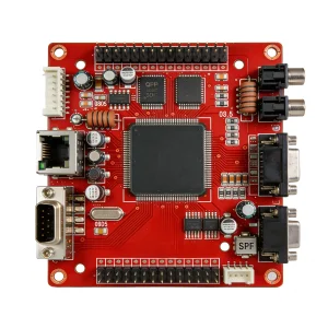
Engineered to withstand rigorous mission-critical environments. Explore our frontline electronic manufacturing products developed across industrial, medical, and security infrastructures.
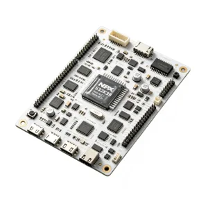
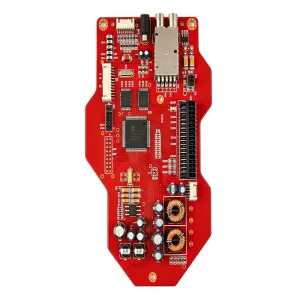
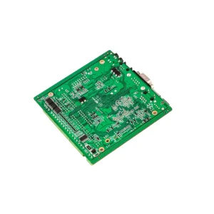
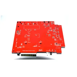

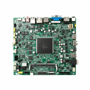
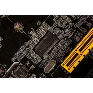
The global electronics engineering paradigm demands higher velocity, end-to-end component traceability, and zero-defect yields. China’s PCB manufacturing ecosystem has evolved from high-volume labor to intelligent, automated smart factories driven by AI-powered SMT lines and closed-loop process automation.
Our intelligent pick-and-place systems handle sub-millimeter packages down to 01005 and micro-BGAs (0.35mm pitch). Optical and 3D X-ray systems (AXI) run automated deep-learning algorithms to detect micro-voids, solder bridging, and tombstoning in real time, delivering near-zero rework cycles.
Full-spectrum traceability is embedded into every PCB lot. From raw laminate pre-preg verification to reel barcode scanning on feeder racks, our manufacturing execution system logs component batch data, reflow oven thermal curves, and test metrics for unmatched audit defensibility.
Shenzhen acts as the primary hardware epicenter of the world. Proximity to major semiconductor brokers, passives distribution centers, and high-precision tooling partners shrinks component lead-times from weeks to hours, neutralizing geopolitical and maritime freight shocks.
A bare circuit board is only as good as its operational reliability under physical, environmental, and thermal extremes. We engineer customized manufacturing pathways across multiple critical application vectors.
Operating under strict ISO 13485 guidelines, we manufacture high-density PCBAs for portable ultrasonography, MRI imaging backplanes, and wearable biosensors. Includes class-3 conformal coating, bio-compatible materials, and comprehensive ion contamination wash testing.
Certified under IATF 16949, our automotive electronics assembly complies with PPAP Level III standards. High-voltage battery management systems (BMS) and vehicle control units (VCU) leverage thick-copper substrates (up to 6oz) to withstand thermal cycling and vibration fatigue.
For smart metering, long-range radar, and remote telemetry, we execute specialized PCB fabrication using Rogers, Taconic, and Teflon hybrid stacks. We manage controlled impedance lines (±5% tolerance) and blind/buried micro-vias for optimal RF signal integrity.
| Technical Capability Metric | Standard Production Tier | Advanced / Aerospace / Medical Tier | Verification & Test Protocol |
|---|---|---|---|
| Layer Count & Substrate Types | 1 - 16 Layers (Standard FR-4, Aluminum) | Up to 64 Layers (Rigid-Flex, Rogers, Ceramic, High-Tg) | Micro-section analysis, TDR impedance test |
| Min. Line Width / Spacing | 3.0 mil / 3.0 mil (0.075mm) | 1.8 mil / 1.8 mil (HDI any-layer via processes) | Automated Optical Inspection (AOI) |
| Fine Pitch & Component Capabilities | 0201 passives, 0.4mm pitch QFP/BGA | 01005 passives, 0.3mm ultra-fine pitch BGA, PoP | 3D X-Ray Inspection (AXI) & Shear Testing |
| Surface Finishes | HASL lead-free, ENIG (Electroless Nickel Immersion Gold) | ENEPIG, Immersion Silver/Tin, Hard Gold Plating | XRF plating thickness verification |
| Functional Validation | Bed-of-Nails In-Circuit Test (ICT) | Custom Boundary Scan, FCT, Flying Probe, Environmental Burn-in | Automated functional logging & cloud reporting |
As AI computing accelerates at the edge, circuit board fabrication is shifting toward semiconductor-grade tolerances. Our multi-year capital investment program addresses emerging packaging paradigms.
Procuring PCB manufacturing from China requires more than cost optimization—it requires rigorous intellectual property safeguards, supply chain transparency, and seamless engineering communications.
Mutual Non-Disclosure Agreements (NDAs) precede file transfers. Design files (Gerber, ODB++, schematic BOMs) are isolated on segregated servers protected by role-based access control, cryptographic hashing, and automated deletion policies.
Our facilities are fully certified across ISO 9001 (Quality), IATF 16949 (Automotive), ISO 13485 (Medical Devices), and ISO 14001 (Environmental). All processes adhere to RoHS, REACH, and Conflict Minerals reporting requirements.
Bridge timezone barriers with our bilingual engineering teams. We offer real-time Design for Manufacturability (DFM) and Design for Testing (DFT) consulting before production, avoiding costly spins and accelerating time-to-market.
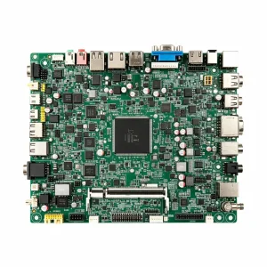
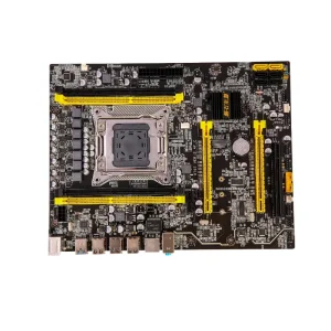
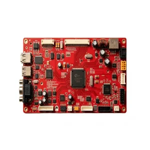
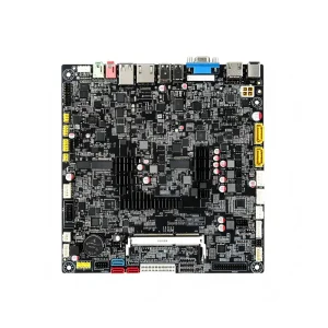
Delivering high thermal efficiency, tight layout tolerances, and extreme lifecycle endurance across mission-critical equipment categories.

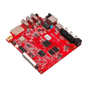
Clear, direct answers for engineering leads, procurement specialists, and global product designers looking to manufacture and assemble boards in Shenzhen.