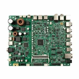
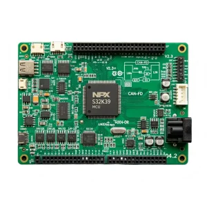
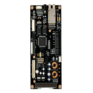
Tier-1 Industrial EMS & SMT Assembly Hub

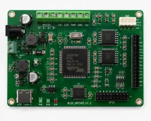
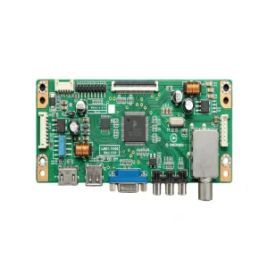
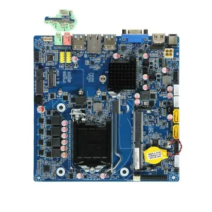
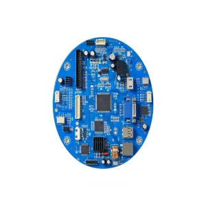
China Make PCB Board Service & Factory

High-precision Bare-board Fabrication, Component Supply Chain Sourcing, Fine-Pitch SMT Assembly, and Full-Cycle Box Build Execution Under IPC Class 2 & 3 Standards.

High-Reliability Product Engineering Portfolio (Part I)

Explore turnkey assemblies built for distributed energy, precision sensor measurement, high-voltage power networks, and industrial IoT controls.
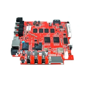

Distributed Power Generation Control System PCB Assembly
High-Quality Distributed Power Generation Control System PCB Assembly Factories, Factory
Configure Assembly
China Radiation Detector PCB Assembly
China Radiation Detector PCB Assembly Factories, Factory
Configure Assembly
High Voltage Power Supply PCB Assembly
High-Quality High Voltage Power Supply PCB Assembly--STHL Manufacturers, Factory
Configure Assembly
OEM Metal Detector PCB Assembly
OEM Metal Detector PCB Assembly--STHL Manufacturer, Manufacturers
Configure Assembly
Water Heater Controller PCB Assembly
High-Quality Water Heater Controller PCB Assembly Service, Factory
Configure Assembly
China GNSS Module PCBA Assembly
China GNSS Module PCBA Assembly--STHL Manufacturer, Factories
Configure Assembly
Direct-Lit LED Backlight PCB Assembly
High-Quality Direct-Lit LED Backlight PCB Assembly--STHL Factories, Factory
Configure Assembly
OEM Air Quality Monitor PCBA Assembly
OEM Air Quality Monitor PCBA Assembly--STHL Manufacturer, Factories
Configure Assembly

Global Commercial Landscape: Why China Dominates Advanced PCB Manufacturing

A systematic perspective on infrastructure density, supply chain clustering, material economics, and quality execution in modern electronics manufacturing.

54.2%
Global PCB Production Market Share
48-Hr
BOM Sourcing Turnaround via PRD Hubs
01005
Micro-SMT Micro-component Precision
100%
MES Traceability & DFM Verification
Ecosystem Colocation Advantage

The Pearl River Delta (Shenzhen, Dongguan, Huizhou) represents an unmatched dense cluster of copper clad laminate (CCL) producers, chemical treatment specialists, precision tooling suppliers, and semiconductor logistics agents. Sourcing passive components, active ICs, and specialty substrates takes hours rather than weeks, preventing the logistics fragmentation typical of decentralized manufacturing sites.

Scalable Agility: Prototypes to Mass Production

Traditional western EMS houses demand rigid MOQ tiers or impose punitive setup surcharges on pilot builds. China's top PCBA factories operate high-mix, low-volume (HMLV) flexible SMT lines concurrently with high-speed automated Siemens/Yamaha production bays. Hardware startups validate Proof-of-Concept (POC) units and seamlessly scale to 100k-unit production without re-qualifying vendors.

Systematic Defect Prevention (Zero-Escape Quality)

Modern Chinese PCB factories have moved far beyond labor arbitrage; operations are driven by automated process controls. Automated Optical Inspection (AOI), 3D Solder Paste Inspection (SPI), In-Line X-ray Inspection (AXI) for BGA/QFN solder voiding, and Flying Probe Testing form standard quality gates ensuring IPC Class 3 compliance for medical, automotive, and industrial applications.

Strategic Sourcing Insight for Hardware Procurement Directors

Selecting a China Make PCB partner requires evaluating engineering depth over nominal per-board quotes. Critical markers include in-house impedance coupon testing, real-time MES traceability dashboards, native component distribution direct line accounts (Arrow, Digi-Key, Mouser, Avnet), and engineering-led DFM reviews that eliminate manufacturing yield traps before copper lamination begins.

Next-Generation PCB Technology Roadmap: 2026–2030

How cutting-edge materials, high-density interconnections, and automated thermal dissipation architectures are shaping the future of global hardware development.

Substrate-Like PCBs (SLP) & mSAP Processes

As micro-controllers and FPGA packages adopt 0.3mm ball-pitch geometries, standard subtractive etching hits trace-width limitations. Leading factories deploy modified Semi-Additive Processes (mSAP) enabling 25/25μm trace width/space lines. This delivers high packaging density, lowers parasitic capacitance, and supports multi-layer HDI stack-ups (up to 4+N+4) for compact edge-AI compute engines.

Thermal Dissipation & Heavy-Copper Substrates

Electrification in automotive powertrains, distributed solar micro-inverters, and high-current industrial charging requires extreme thermal stability. Advanced PCB engineering integrates 3oz to 6oz heavy copper, ceramic substrates (AlN/Al2O3), embedded copper coins, and insulated metal substrates (IMS) to direct thermal loads away from critical switching semiconductors without bulky heat-sinks.

High-Frequency Low-Loss Dielectrics (RF/mmWave)

Next-gen 5G mmWave base stations, satellite radar, and automotive LiDAR require tight impedance control (±5%) and low dielectric loss. Factories combine PTFE, hydrocarbon ceramics, and high-frequency Rogers/Taconic laminates with standard FR-4 prepregs in hybrid multi-layer constructions to balance high-speed signal integrity with commercial assembly cost.

Macro Turnkey Architecture: From Gerber & BOM to Qualified Box Build

A rigorous, closed-loop engineering process designed to eliminate risks across every stage of the electronics manufacturing lifecycle.

Phase 1: DFM/DFA Digital Twin Validation

Before laser direct imaging (LDI) exposes copper panels, senior CAM engineers review your design against 40+ manufacturing rules. This check covers aspect ratio tolerances, acid-trap geometries, annular ring integrity, thermal relief balancing, component shadowing during reflow, and solder mask bridges to ensure flawless production yields.

Phase 2: Global Sourcing & Counterfeit Screening

Component integrity dictates hardware reliability. Our incoming quality control (IQC) inspects passive reels and IC packages under high-power optical microscopes, decapsulation test benches, and X-ray fluorescence (XRF) analyzers to catch date-code mismatches, remarking, and terminal oxidation before parts hit the feeder racks.

Phase 3: Dual SMT / DIP Assembly & Automated Testing

Surface-mount bays equipped with 10-zone nitrogen reflow ovens run solder profiles tuned to thermal masses. In-circuit testing (ICT) verifies passive component values and short/open nets. Functional test jigs (FCT) then simulate operating environments, running live firmware, checking analog rails, and validating RF protocols under load.

Mission-Critical Hardware & Subsystem Assemblies (Part II)

Turnkey assemblies built to ISO 13485 medical, high-voltage industrial, optical lighting, and navigational aerospace specifications.
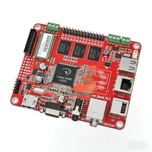
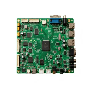
Battery Charger PCB Assembly
High-Quality Battery Charger PCB Assembly Manufacturers, Service
Configure Assembly
OEM Webcams PCBA Assembly
OEM Webcams PCBA Assembly--STHL Manufacturer, Service
Configure Assembly
Inertial Navigation System PCBA Assembly
High-Quality Inertial Navigation System (INS) PCBA Assembly--STHL Manufacturers, Service
Configure Assembly
China Medical PCBA Application
China Medical PCBA Application: Precision and Reliability for Healthcare Devices Manufacturer, Factories
Configure Assembly
China Repeater PCB Assembly
China Repeater PCB Assembly Service, Factory
Configure Assembly
OEM Medical Power Supply PCB Assembly
OEM Medical Power Supply PCB Assembly--STHL Manufacturers, Service
Configure Assembly
Medical Imaging Workstation PCB Assembly
High-Quality Medical Imaging Workstation PCB Assembly--STHL Manufacturers, Service
Configure Assembly
LED Ceiling Panel Light PCB Assembly
OEM LED Ceiling Panel Light PCB Assembly--STHL Manufacturer, Service
Configure Assembly

Engineering FAQ: Direct Answers for Procurement & Hardware Engineers

Comprehensive details on engineering reviews, BOM sourcing verification, quality certifications, and global IP protection.

How do you guarantee electronic components are authentic and free from gray-market counterfeit risks?
Our procurement operates strictly through direct manufacturer pipelines and franchised Tier-1 global distributors (Arrow, Avnet, Digi-Key, Mouser, Farnell, WPG). When hard-to-find or legacy parts are required, incoming lots run through an intensive multi-gate verification process at our on-site laboratory. This includes external visual inspection under 50x magnification to spot scrape marks, pin re-tinning, or chemical etching, followed by XRF testing for RoHS elemental compliance, real-time X-ray verification of internal lead-frame bonds, and acetone swipe tests to reveal re-topped surface coatings. Every reel receives an internal UID connected to our MES system for full lot traceability.
What tolerances can your SMT lines hold on fine-pitch BGAs, QFNs, and micro-passives?
Our automated surface-mount assembly lines run modular Yamaha and Panasonic mounters delivering component placement accuracy down to ±0.025mm (±25μm) at Cpk ≥ 1.33. Our capabilities support ultra-miniature 01005 passives, 0.3mm ball-pitch ultra-fine BGAs, PoP (Package-on-Package), and fine-pitch QFNs. Solder deposit height and volume are validated 100% via inline 3D SPI systems using multi-frequency phase-shift profiling. This caught volume variances, bridging, and solder-mask registration errors before components ever hit the reflow oven.
How is intellectual property (IP), firmware security, and design data protected in your factory?
Data security is backed by legal and network safeguards. We execute binding NDAs prior to opening any CAD files or BOM archives. Gerber, schematic, and drill data are stored on isolated, encrypted internal servers accessible only to the assigned project CAM and DFM team. In programming areas, production firmware is flashed using closed-loop, encrypted flash programmers that prevent raw hex code extraction. USB drives are restricted across factory workstations, and programming cells operate under continuous CCTV surveillance. We also support end-customer HSM secure key generation workflows for automotive and IoT devices.
Can your facility transition seamlessly from prototype validation to high-volume assembly?
Yes. We eliminate the friction of migrating between prototype quick-turn shops and mass-production houses. Fast-turn NPI lines handle low-volume verification builds (2 to 50 units) without rigid minimum order quantity (MOQ) thresholds. The tooling assets, thermal reflow recipes, stencil laser apertures, and test fixtures developed during NPI are digitally archived in our MES. Once your pilot build passes functional and regulatory testing, production scales directly to our high-speed automated lines without re-spinning the process setup or repeating qualification loops.
Which environmental, quality, and industry-specific certifications govern your operations?
Our facilities operate under four primary third-party verified quality management systems: IATF 16949 (automotive defect prevention and failure mode control), ISO 13485 (medical device electronic systems and traceability), ISO 9001 (general quality systems), and ISO 14001 (environmental management). Bare boards comply with IPC-6012 Class 2 and Class 3, while assembly operations are governed by IPC-A-610 Class 2 and Class 3 work instructions overseen by in-house certified IPC trainers (CIT).
What specific files are required to obtain a comprehensive, engineering-backed DFM quote?
To prepare a comprehensive DFM and manufacturing quote, please provide: (1) Gerber files in RS-274X format or native ODB++ archives including layer stack-up details; (2) A complete Bill of Materials (BOM) in Excel format with component designators, full manufacturer part numbers (MPN), descriptions, and recognized second-source alternatives; (3) Centroid / Pick-and-Place data containing X-Y coordinates, rotation, and layer orientation; (4) Fabrication drawings detailing copper thickness, solder mask color, surface finish (ENIG, HASL, Immersion Silver/Tin), and impedance targets; and (5) Functional test instructions along with custom fixture schematics where applicable. Quotes with complete DFM reviews are returned within 24 to 48 hours.