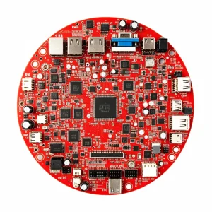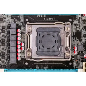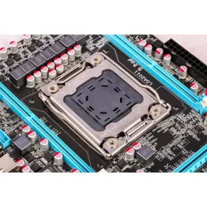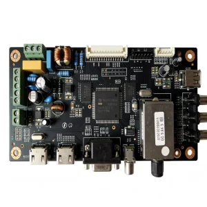
Explore production-grade multilayer PCBA projects certified for critical automotive, avionics, industrial safety, and smart mobile endpoints.


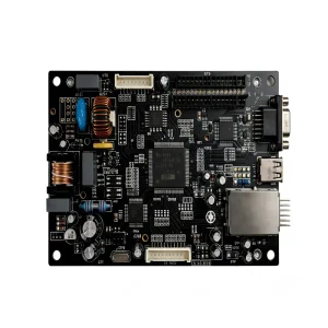
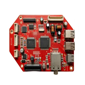
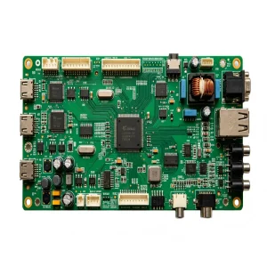
The electronic hardware landscape is rapidly shifting toward dense, multi-functional, and thermally robust architectures.
The transition to higher frequencies (sub-6 GHz and millimeter-wave) demands multilayer boards with tight impedance tolerances (±5%), low-loss substrates (Megtron 6, Rogers), and precise layer-to-layer registration to mitigate skin effect and dielectric losses across cloud networking switches and server accelerator modules.
Automotive power electronics, ADAS perception arrays, and Battery Management Systems (BMS) require high copper weight layers (3oz to 6oz) merged with signal traces. Advanced thermal dissipation methods such as buried copper coins and thermal vias prevent junction overheating under stringent IATF 16949 conditions.
Medical wearables, portable instrumentation, and enterprise IoT hardware increasingly deploy Any-Layer HDI (microvias from 1-N layers). Staggered, stacked, and copper-filled laser microvias allow ultra-fine BGA ball pitches down to 0.35 mm, maximizing functional density within minimal spatial footprints.
Harnessing the world's most concentrated electronics hardware ecosystem to deliver unmatched lead-time compression and supply chain resilience.
Located in Bao'an, Shenzhen, STHL leverages a 1-hour sourcing radius for specialized laminates (Shengyi, ITEQ, Rogers), precision stencils, custom tooling, and standard passives, minimizing standard supply chain delays.
Our 50+ on-site engineering staff evaluates IPC-A-600/610 compliance prior to production, checking thermal reliefs, annular rings, aspect ratios, and solder bridge clearances to eliminate costly engineering holds.
Proprietary MES architecture maps every single reel, SMT nozzle, reflow thermal profile, and automated visual inspection (AOI/AXI) result to a unique board serial barcode, ensuring medical-grade traceability.
Seamlessly transition from quick-turn, high-mix prototypes to high-volume multi-panel runs on the exact same calibrated Yamaha and Panasonic pick-and-place lines without configuration mismatches.
Verified manufacturing parameters for engineering qualification and procurement audits.
| Capability Parameter | Standard Prototype Limit | Advanced Production Capability | Target Engineering Standard |
|---|---|---|---|
| Layer Count Range | 2 – 16 Layers | Up to 48 Layers (Rigid / Rigid-Flex) | IPC-6012 Class 2 / Class 3 |
| HDI Microvia Architecture | 1+N+1 Laser Drilled | Any-Layer HDI (ELIC), Stacked Copper-Filled | IPC-2226 Type III to Type VI |
| Min. Trace Width / Spacing | 3.5 mil / 3.5 mil (0.089 mm) | 2.0 mil / 2.0 mil (0.05 mm) | Controlled Impedance (±5%) |
| Drill Aspect Ratio | 8:1 Through-Hole | 12:1 Through-Hole; 1:1 Microvia | Laser UV / Mechanical CNC |
| Laminate Base Materials | Standard FR-4 (Tg 130-140°C) | High Tg FR4 (>170°C), Rogers, Nelco, Polyimide, Al-Core | RoHS / REACH Compliant |
| Surface Finishes | HASL / Lead-Free HASL | ENIG, ENEPIG, Immersion Silver/Tin, Hard Gold Plating | IPC-4552 (ENIG thickness audited) |
| SMT Component Placement | 0402 Passives, 0.5mm IC Pitch | 01005 Passives, 0.35mm Micro-BGA, PoP (Package-on-Package) | IPC-A-610 Class 3 Workmanship |
| Inspection & Verification | Automated Optical Inspection (AOI) | 3D SPI, 3D AOI, 2.5D/3D X-Ray (AXI), In-Circuit & FCT | 100% Netlist Flying Probe / E-Test |
How global purchasing managers optimize BOM risk, lead-time variance, and compliance overhead.
Separating bare-board fabrication, passives procurement, and SMT assembly across distinct entities exacerbates friction, adds multiple logistics tariffs, and obscures root cause accountability during solder bridging or delamination events. Complete turnkey integration mitigates supply liability.
Sudden lifecycle shifts (EOL/PCN) disrupt production cycles. STHL maintains direct API connectivity with verified semiconductor channels (Mouser, Digi-Key, Arrow, Avnet) paired with audited Asian component brokers to identify drop-in pin-compatible alternatives and prevent line standstills.
Confidential hardware development necessitates air-gapped test programming cells, strict bilateral non-disclosure protocols (NDA), and isolated local database servers. Intellectual property is guarded continuously from initial Gerber validation through firmware flashing.
Actionable answers to technical, commercial, and quality assurance inquiries from international hardware engineers.
Engineered to operate reliably under extreme environments, high-voltage conditions, and continuous operation.