
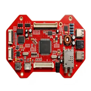
Engineered to IPC-A-610 Class 3 specifications with rigorous SPI, 3D AOI, and continuous X-ray validation.
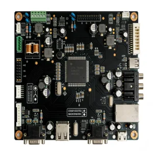
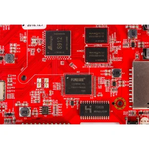
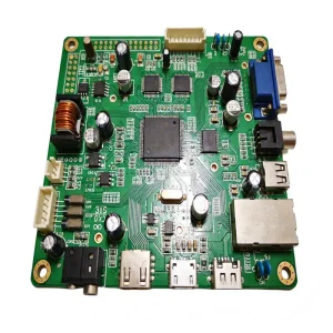
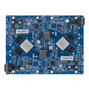
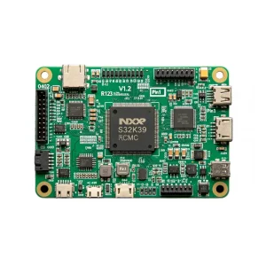
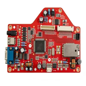
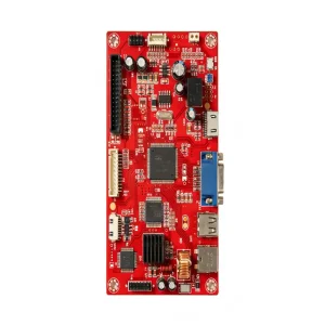
The transition from conventional contract assembly to integrated Electronic Manufacturing Services (EMS) demands unprecedented technical rigor and end-to-end traceability.
Mounting tolerances down to ±15μm enable zero-defect population of 01005 passives and ultra-fine-pitch 0.3mm micro-BGAs. Our automated SMT lines utilize nitrogen-atmosphere reflow ovens with 10 thermal heating zones, eliminating solder bridging and voiding while optimizing intermetallic compound (IMC) formation across mission-critical circuits.
Defect prevention relies on multi-layer verification. Integrating Automated Optical Inspection (AOI), 3D Computed Tomography (CT) X-ray, and automated In-Circuit Testing (ICT) ensures every hidden joint beneath BGA, QFN, and land-grid-array (LGA) components complies with IPC Class 3 void ratio standards (<15%).
Beyond surface mount operations, modern PCBA manufacturing requires end-to-end integration: early-stage Design for Manufacturability (DFM) reviews, automated firmware flash operations, precision conformal coating against harsh atmospheric conditions, and system-level mechanical enclosure assembly (Box Build).
Operating within Shenzhen's premier electronics corridor, our infrastructure combines hyper-localized component access with digitized smart manufacturing.
| Dimension | Conventional Contract Manufacturer | Factory 4.0 Integrated EMS (STHL Standard) | OEM Procurement Value |
|---|---|---|---|
| BOM Sourcing Speed | Manual RFQ rounds (3-4 weeks) | Direct API link to 100+ authorized global distributors | Shortened quote cycles down to 24-48 hours |
| Traceability | Batch-level paper routing | Unique 2D matrix barcode serialized per PCBA into MES | Full lot-level auditing from chip wafer to field return |
| DFM Evaluation | Post-order reactive checking | Pre-production automated Valor DFM/DFA engineering analysis | Eliminates re-spins, reducing tooling costs by ~30% |
| Scalability Curve | Rigid MOQs, high line changeover delays | Agile lines supporting prototype batches through mass runs | Zero MOQ penalty; seamless bridge from NPI to volume |
Each industry poses unique environmental stresses, validation standards, and regulatory landscapes. Our manufacturing cells are configured specifically for these verticals.
Fabrication under ISO 13485 standards. Guaranteed cleanroom assembly, strict biocompatible materials verification, multi-stage bio-burden control, and validation reports supporting FDA and CE-MDR Class II/III submissions.
Certified under IATF 16949. Rigorous APQP, PPAP Level 3 documentation, high thermal cycling testing (-40°C to +125°C), and copper-inlay power substrates for Battery Management Systems (BMS) and ADAS sensor arrays.
Heavy-duty layouts with thick copper (up to 6oz) to carry continuous high currents. Superior transient surge suppression, conformal robotic potting, and vibration tolerance compliant with IEC 60068 standards.
IPC Class 3 assembly protocols, high-Tg polyimide base laminates, ENIG / immersion silver surface finishes, and zero-gravity/vacuum outgassing risk mitigation through specialized thermal cure profiles.
Impedance-controlled RF substrates (Rogers, PTFE, Megtron) optimized for 5G, Wi-Fi 6E, and UWB protocols. Automated RF shielding can placement and spectrum testing up to sub-6GHz frequencies.
High-dielectric breakdown substrates designed for high-voltage solar microinverters, battery energy storage systems (BESS), and power distribution units (PDU) subject to extensive thermal dissipation demands.
As electronic systems shrink while handling faster data transfer and higher thermal loads, our production engineering roadmap remains ahead of market shifts.
Scaling to sub-25μm trace/space parameters with laser-drilled microvias (any-layer HDI). Facilitating multi-die packaging, silicon-in-package (SiP), and dense computing platforms without signal-reflection compromises.
Embedding discrete capacitors, resistors, and miniaturized dies inside the inner layers of the PCB substrate. This shortens signal loops, virtually eliminates parasitic inductance, and frees up board surface space by 35%.
Integrating direct-bonded copper (DBC), insulated metal substrates (IMS), and hybrid ceramic-FR4 multilayers. Designed specifically to handle gallium nitride (GaN) and silicon carbide (SiC) power semiconductor arrays.
International engineering partnerships require absolute legal certainty, institutional quality controls, and borderless technical dialogue.
Design intellectual property is secured through strict air-gapped engineering networks, role-based access controls, and legally binding international Non-Disclosure Agreements (NDAs) before design files are received. Source firmware and cryptographic key materials are handled in physically secure flashing chambers.
Eliminate communication overhead and cultural disconnect. Our in-house engineering team delivers live technical consultations in fluent English, providing real-time Design for Manufacturability (DFM) and Design for Assembly (DFA) feedback directly across Europe and Americas timezones.
Benefit from seasoned supply chain operations with direct Door-to-Door (DDP) shipments to over 90 countries. Handled through bonded logistics facilities with complete documentation (RoHS, REACH, UL 94V-0, Certificates of Origin) for friction-free customs clearance.




Evaluating Chinese PCBA manufacturers extends well beyond bare board unit costs. Sophisticated procurement managers evaluate risk, yield stability, and end-of-life component management.
Component sourcing through verified franchised distributors (Arrow, Avnet, DigiKey, Mouser) alongside audited original component manufacturers. In-house verification laboratories inspect incoming active silicon via decapsulation, XRF metallurgic analysis, and pinout electrical tests.
Proactive lifecycle tracking identifies obsolete or long-lead silicon months ahead of wafer shortages. Our engineering team suggests form-fit-function (FFF) pin-compatible drop-ins, complete with re-engineered layout suggestions and updated firmware testing.
Through statistical process control (SPC) on solder paste volumes and real-time reflow profiling, our factory maintains a production line First-Pass Yield exceeding 98.8%, dramatically curbing rework cycles and latent field defect risks.
Detailed technical, contractual, and quality answers to streamline your supplier qualification process.
Our supply chain operates exclusively with Tier-1 franchised distributors (Digi-Key, Mouser, Arrow, Avnet) and verified original component manufacturers (OCM). For every bill of materials (BOM), full Certificates of Conformance (CoC) and lot-level traceability are maintained. If spot-market sourcing is requested to resolve long leads, our incoming QC lab conducts X-ray leadframe inspection, solvent marking tests, and decapsulation before any reel enters the SMT feeders.
For an accurate and actionable turnkey quote within 24 to 48 hours, please supply: Gerber files in RS-274X or ODB++ format, a structured BOM list specifying manufacturer part numbers (MPN), footprints, and reference designators, a centroid (Pick-and-Place X-Y coordinate) file, fabrication notes defining layer stackup and surface finish (ENIG, HASL, OSP), and a testing specification document outlining functional testing steps.
Our SMT pick-and-place lines populate micro-components down to 01005 (imperial) and micro-BGAs down to a 0.3mm ball pitch. Solder deposition is continuously measured via high-speed 3D SPI. Solder joints beneath BGAs and bottom-terminated components (QFN/LGA) undergo 100% automated 3D X-ray inspection to guarantee voiding levels stay well below IPC Class 3 limits.
Yes. We enforce a zero Minimum Order Quantity (no MOQ) framework. Hardware development teams can order 5 to 50 boards for initial functional bench testing and regulatory pre-compliance runs. Once validated, your build moves to our high-speed, multi-feeder automated lines using identical DFM profiles, component feeder maps, and MES work order setups without re-engineering delays.
Confidentiality is protected under enforceable non-disclosure agreements before design files are transferred. Engineering workstations operate in an access-restricted, air-gapped subnet where design data cannot be copied to external USB media. Flashing of hex/bin firmware files is performed through encrypted automated programmers, preventing operator visibility into proprietary machine code.
For rapid NPI prototypes, boards can be fabricated, assembled, and tested within 3 to 7 working days once parts arrive at the factory. Standard production batches typically take 15 to 25 business days, dictated primarily by custom PCB fabrication stackup complexity and component procurement lead times. Express component air-freight and priority tooling options are readily available.
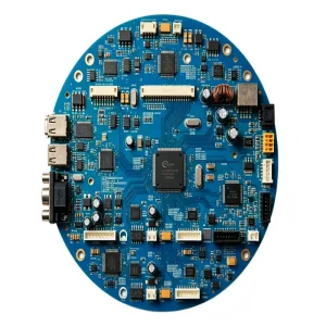
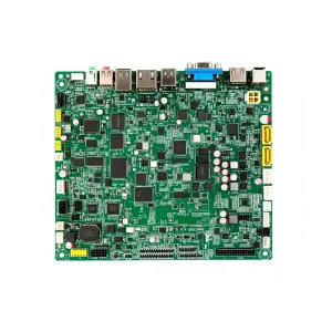
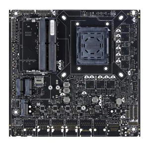
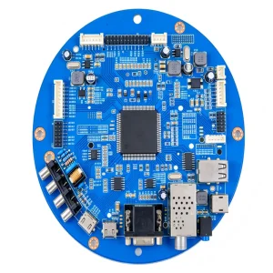
Explore additional mission-critical electronics manufactured in our Shenzhen production facility.

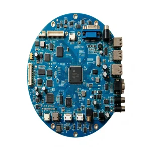
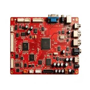

Submit your Gerber data and Bill of Materials to our engineering team. Receive an exhaustive DFM feedback analysis, component lifecycle evaluation, and firm production pricing within 24 hours.