As mission-critical electronics evolve toward extreme miniaturization, high-frequency signal integrity, and harsh-environment durability, choosing an authentic Chinese turnkey PCBA manufacturer is no longer merely a procurement exercise. It is a foundational strategic partnership requiring deep Design for Manufacturability (DFM) verification, zero-defect quality systems, and an unshakeable supply chain.
Operating 7 automated SMT lines equipped with high-speed Yamaha and Fuji pick-and-place systems, our Shenzhen manufacturing facility handles high-density, double-sided placements down to 01005 (0402 metric) chips, 0.3mm pitch micro-BGA packages, Package-on-Package (PoP), and ultra-fine QFNs. Nitrogen-purged 10-zone reflow soldering ensures solder voiding is consistently controlled below 10%, satisfying rigorous automotive and aerospace durability criteria.
From multi-layer bare PCB fabrication (up to 48 layers, Any-Layer HDI, Rogers, and Rigid-Flex) to automated BOM component procurement through franchised distributors, through-hole selective wave soldering, conformal coating, IC burning, and final box-build mechanical integration. Work orders are monitored live through our proprietary ERP and MES tracking engines to ensure batch serialization and full bill-of-materials traceability.
Explore representative turnkey PCBA manufacturing deliverables manufactured in our Shenzhen facility, serving Tier-1 OEMs worldwide across environmental, medical, computing, and automotive sectors.

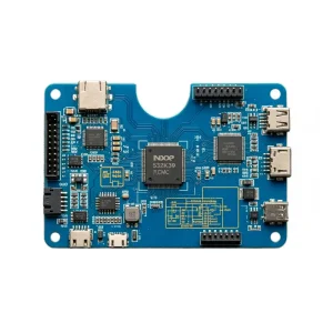
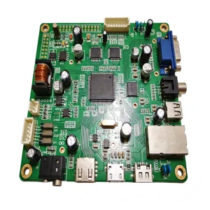
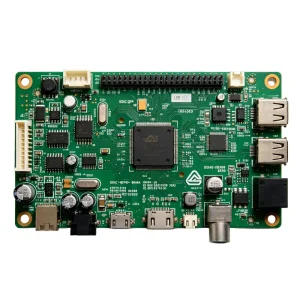
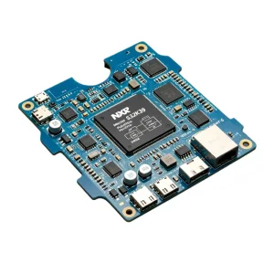
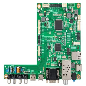
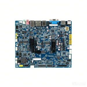
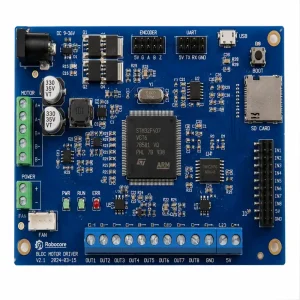
Our manufacturing parameters are continually calibrated against IPC-A-610 Class 2 and Class 3 criteria, catering to ultra-compact consumer electronics as well as mission-critical industrial controllers.
| SMT Placement Accuracy | ±0.035mm (35µm) at 3σ for fine-pitch QFP/BGA; ±0.025mm for standard discrete passives. |
|---|---|
| Component Package Range | Passive chips down to 01005 (0402 metric), 0201, 0402 up to 54mm x 54mm connectors; BGA/LGA down to 0.3mm pitch. |
| PCB Dimensions | Min: 50mm x 50mm; Max: 610mm x 1200mm (Ultra-long LED panels and industrial backplanes). |
| Board Layer Count & Substrates | 1 to 48 Layers; Standard FR-4, High-Tg (TG170/TG180), Halogen-Free, Rogers, PTFE, Polyimide Flex, Rigid-Flex, Aluminum, Ceramic Core. |
| Soldering Technologies | Lead-Free (RoHS) reflow soldering with Nitrogen purging, wave soldering, selective robotic soldering, and vapor phase options. |
| Testing & Quality Verification | 3D SPI (Solder Paste Inspection), Inline 3D AOI (top/bottom), 2D/3D Automated X-ray Inspection (AXI), Flying Probe ICT, Custom Bed-of-Nails Functional Testing (FCT), Thermal Shock, and Burn-in chambers. |
| Specialty Finishing Services | Automated Conformal Coating (acrylic, polyurethane, silicone), Potting, Ultrasonic plastic welding, Cable Harness fabrication, Metal/Plastic CNC box-build integration. |
| Certifications & Accreditations | IATF 16949 (Automotive), ISO 13485 (Medical), ISO 9001:2015, ISO 14001:2015, UL Underwriters Laboratories, IPC-WHMA-A-620. |
Beyond simple labor economics, the Greater Bay Area represents the world's most concentrated, resilient, and responsive electronics hardware ecosystem.
Within a 30-kilometer radius of our Bao'an facility lies access to over 500,000 qualified electronic component line items. From franchised authorized distributors (Arrow, Avnet, DigiKey, Mouser) to factory-direct passives (Murata, TDK, Yageo), our procurement lead-times average 60% faster than western regional EMS providers.
Hardware innovation cannot tolerate 8-week NPI prototype cycles. We support agile hardware design teams with 24-to-48-hour quick-turn PCBA prototypes without minimum order quantity (MOQ) restrictions. Once validated, designs scale seamlessly into multi-thousand mass-production runs on identical SMT production parameters.
Component obsolescence, long allocation queues, and tariff pressures frequently stall electronic builds. Our team of 50+ engineers executes systematic BOM health analyses, recommending pin-compatible, automotive-grade Asian second-source semiconductors that reduce unit BOM cost by 15%–40% without compromising MTBF.
Electronic assemblies face extreme thermal cycles, continuous mechanical vibration, and electromagnetic interference depending on their deployment terrain. Here is how our localized engineering addresses core industrial realities.
Certified under ISO 13485, our cleanroom SMT environments produce boards for anesthesia workstations, patient monitors, and clinical diagnostic terminals. Utilizing automated optical and X-ray inspection, we ensure non-destructive solder validation, ion contamination testing, and IPC Class 3 zero-failure reliability.
Governed by IATF 16949, we engineer PCBA assemblies for heads-up displays (HUD), battery management systems (BMS), motor controllers, and onboard telematics. Advanced thermal via arrays, thick-copper copper-inlay substrates, and automated potting guarantee survivability from -40°C to +125°C.
Power distribution units (PDUs), wastewater telemetry nodes, and municipal wireless gateways demand decadal field life. We deploy dual-cure conformal coatings, anti-sulfuration chip resistors, and vacuum-sealed potting to insulate critical traces from moisture, hydrogen sulfide, and galvanic corrosion.
As semiconductor lithography shrinks and power densities climb, PCB assembly converges with semiconductor packaging. Here is our technological development trajectory guiding global hardware leaders into the next decade.
Integrating deep-learning computer vision across solder paste printing (SPI) and placement stages. Real-time machine-to-machine (M2M) feedback automatically compensates stencil offset and squeegee pressure dynamically, eradicating solder bridging and insufficient wetting before reflow ovens are triggered.
Bridging HDI PCBs and IC substrates with mSAP (modified Semi-Additive Process) trace geometries down to 25/25µm line/space. Our future lines embed passive capacitors and resistors directly within the inner laminate layers, slashing electromagnetic footprint and freeing up 40% surface area.
Pioneering Bismuth-Tin (Sn-Bi) low-temperature soldering alloys with peak reflow temperatures around 170°C–190°C. This breakthrough slashes SMT energy consumption by 28%, prevents thermal warpage in ultra-thin substrates, and safeguards temperature-sensitive optical and MEMS sensor dies.
We operate as a transparent manufacturing arm for western enterprises. Legal protection, air-gapped data workflows, and compliance certifications assure frictionless international deployment.
Your firmware, Gerbers, and schematics represent your company’s core enterprise value. We execute internationally recognized NDAs governed under international or local jurisdiction prior to receiving your engineering files, strictly siloing project data within encrypted, air-gapped servers.
Every bare board, solder alloy, flux chemistry, and passive component placed in our facility complies with EU RoHS 3 (Directive 2015/863) and REACH substance restrictions. We provide verified chemical declarations, flame-retardant UL94V-0 listings, and Conflict Mineral Reporting Templates (CMRT).
No language barriers or delayed email threads. Overseas clients are assigned a dedicated English-fluent Program Manager and Senior SMT DFM Engineer, ensuring real-time resolution on component lead-times, engineering inquiries (EQs), and shipment customs documentation.
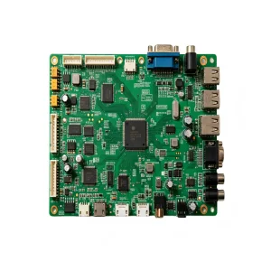
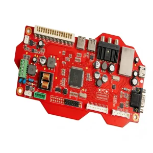
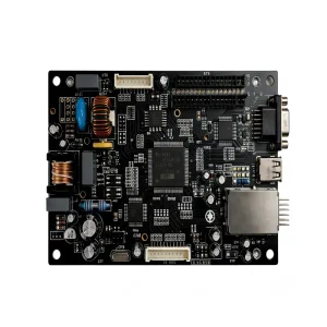
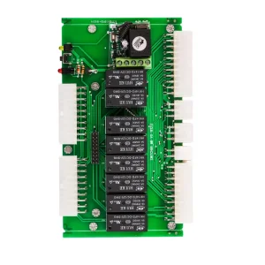
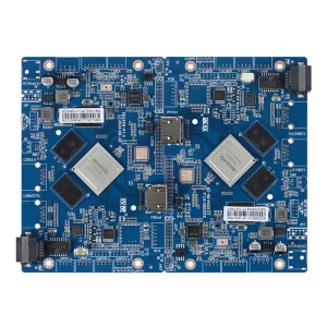
Discover additional precision-assembled assemblies produced for security, industrial communications, energy storage, consumer electronics, and aerospace control applications.


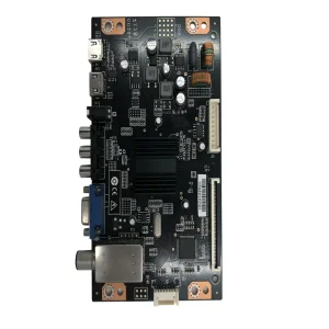
Detailed engineering answers addressing technical requirements, quality control gates, counterfeit component mitigation, and export operations.
Connect directly with STHL senior manufacturing engineers. Send your Gerber files and Bill of Materials (BOM) under NDA for an actionable DFM feasibility audit and comprehensive turnkey quotation within 24 hours.
