
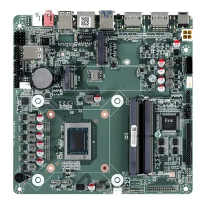
Explore production-grade board systems built to rigorous IPC Class II and Class III workmanship standards.


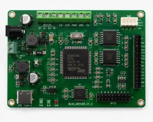

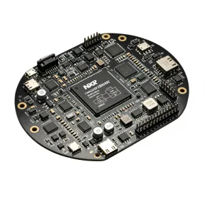
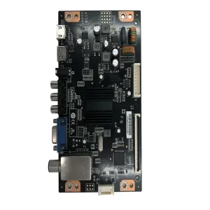
The electronic manufacturing services ecosystem is undergoing a structural paradigm shift driven by high-density interconnects, localized supply-chain reshoring pressures, and automotive electrification.
Modern electronic engineering requires rapid BOM component procurement. China's Greater Bay Area houses over 70% of upstream electronic component fabricators, micro-passive component houses, and substrate manufacturers within a 50 km logistics radius. This physical proximity cuts supply chain lead times from weeks to single-digit hours, ensuring quick-turn prototype builds and mass volume scaling without the risk of extended logistics choke points.
With the rise of Autonomous Driving (ADAS), high-voltage onboard chargers (OBC), and vehicle control units (VCU), the PCBA industry must adhere to zero-defect protocols. Certifications such as IATF 16949 are non-negotiable. Modern automotive lines demand Automated Optical Inspection (AOI), 3D Solder Paste Inspection (SPI), and high-resolution X-ray inspection for bottom-terminated components like BGA and QFN architectures.
The convergence of edge AI computing, wearables, and IoT has led to extreme package miniaturization, requiring ultra-fine pitch placement (01005 passives and 0.3mm pitch BGAs). Modern factory workflows require closed-loop nitrogen reflow ovens, automated conformal coating lines, and integrated IC programming to deliver turnkey durability against thermal cycling and mechanical shock.
Operational data and manufacturing benchmarks from our Bao'an, Shenzhen advanced PCBA facility.
How tier-1 PCBA assembly factories navigate the future of microelectronics, smart robotics, and high-frequency communication.
Moving beyond conventional rule-based algorithms, integrated AI vision engines analyze post-reflow solder joint meniscus volume, detecting micro-voiding and bridging defects with near-zero false-positive rates, ensuring IPC-A-610 Class 3 compliance across high-volume production runs.
With 5G Advanced and emerging 6G infrastructure, PCBA capabilities are expanding to support high-frequency substrates (PTFE/Rogers, Megtron 6, and hybrid ceramic cores) with controlled differential impedance tolerances kept within ±5%.
Every component batch, reflow thermal profile, and technician sign-off is digitally tagged via QR codes laser-etched onto the PCB. This ensures complete traceability from incoming raw components through functional testing.
Engineered hardware manufacturing architectures serving regulated global sectors.
Manufacturing of Battery Management Systems (BMS), On-Board Chargers (OBC), and motor inverter controllers. Standardized on heavy copper boards (3oz to 6oz), automated underfill for mechanical dampening, and high-voltage isolation barrier testing up to 3000V DC.
Fabrication under certified ISO 13485 cleanroom protocols. Specialized in ultrasound transducer boards, patient monitoring instrumentation, and ventilator control units featuring rigorous component life-cycle tracking and conformal coating to protect against bio-chemical cleaning agents.
Assemblies engineered for 24/7 continuous operation under harsh shop-floor environments. Designed with high-Tg FR-4, thick gold plating (ENIG/Hard Gold), transient voltage suppressors, and custom box-build integration inside IP67/IP68 ingress-rated chassis.
Production assemblies delivered for international instrumentation, smart building, and industrial clients.
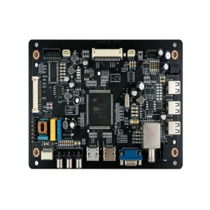
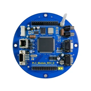
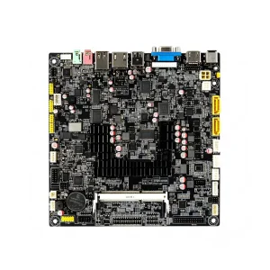
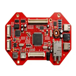
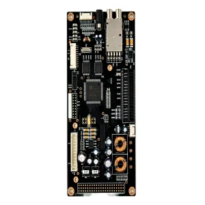
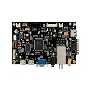
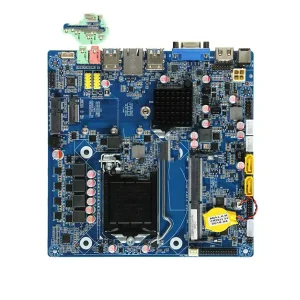
Clear, direct answers for engineering managers and strategic procurement directors evaluating turn-key PCBA manufacturing partners.
Leading tier-1 facilities enforce a zero-tolerance incoming material quality assurance (IQC) protocol. Purchases are channeled strictly through authorized franchised distributors (such as Digi-Key, Mouser, Arrow, Avnet, and original component manufacturers). Sourcing is supplemented with incoming decapsulation, marking inspection under high-magnification optical microscopes, and XRF elemental composition verification to eliminate counterfeit risks.
To provide a detailed quote within 24 hours, the engineering team requires: Gerber files (RS-274X or ODB++ format), an organized Bill of Materials (BOM) detailing manufacturer part numbers (MPN) and reference designators, a Pick-and-Place (Centroid / XY data) file, PCB fabrication specifications (layer count, base material, thickness, copper weight, surface finish), and a Functional Testing Specification (FTS).
Before bare-board fabrication or stencil tooling begins, our production engineers perform a full DFM/DFA review. We evaluate trace clearance, thermal relief pad sizing, solder bridge likelihood, via-in-pad requirements, component spacing for automated pick-and-place nozzles, and shadow effects during reflow soldering. This preliminary audit consistently eliminates costly revisions prior to pilot production.
We execute legally binding bilateral Non-Disclosure Agreements (NDAs) prior to receiving proprietary Gerber or schematic files. Internally, strict file-access control protocols restrict firmware access exclusively to certified test engineers on an isolated, air-gapped test-programming network, preventing unintended distribution.