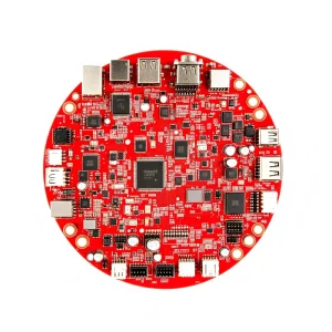
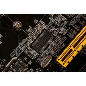
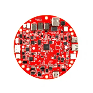
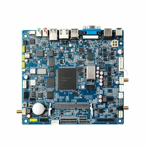
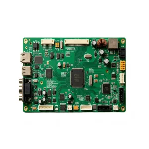
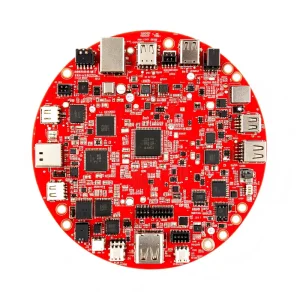
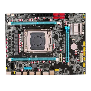
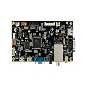
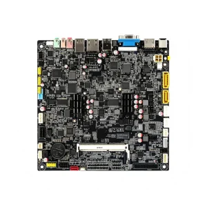
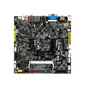
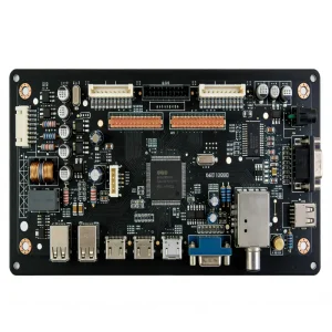
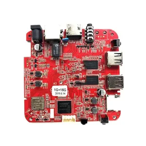
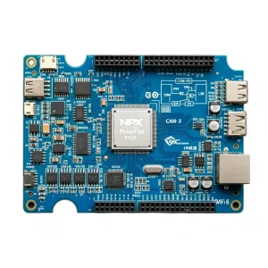
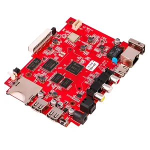
Verified production runs designed for high thermal stability, high reliability, and mission-critical electronics deployment.
Leveraging deep industrial clusters in Shenzhen to provide frictionless contract manufacturing, end-to-end component traceability, and automated precision assembly.
Situated at the nexus of the Pearl River Delta electronics cluster, STHL secures tier-1 factory pricing and direct component pipelines from 100+ vetted distributors and semiconductor houses. This mitigates lead-time volatility and eliminates grey-market component risks.
Every PCBA project is digitized through real-time MES and ERP architecture. From reflow thermal profiling and solder paste inspection (SPI) data to serialized component reels, our factory floor tracks each micro-operation for strict audits and zero-defect initiatives.
Overcoming the conventional friction between NPI (New Product Introduction) and mass volume runs, STHL offers low-to-high volume transitions on the same standardized SMT/THT high-speed mounters, requiring no MOQ and preserving engineering fidelity.
Custom substrate engineering, thermal dissipation technologies, and extreme-environment performance tailored to Tier-1 industrial demands.
IATF 16949-certified manufacturing pipelines supporting heavy-copper substrates, high-voltage battery management systems (BMS), radar micro-modules, and robust onboard chargers with strict AOI and X-ray verification.
Manufactured under ISO 13485 protocols, delivering clinical-grade consistency, anti-interference layout execution, and high-density interconnect (HDI) solutions for patient-critical monitors and diagnostics.
Conformal coating, thick copper inner-layers, and high-Tg substrates designed to withstand extreme thermal fluctuations, vibration, and electro-magnetic transients in PLCs, motor drivers, and smart gateways.
High-frequency RF circuit production utilizing Rogers and PTFE hybrid laminates, low-loss dielectric controls, and controlled-impedance lines calibrated for 5G transmitters, switches, and OLT systems.
Continuous investment into ultra-dense interconnects, advanced substrate metallization, and automated test execution to match semiconductor breakthroughs.
Equipped with high-accuracy dual-lane modular mounters capable of reliable high-speed placement down to 01005 passives and 0.3mm micro-BGA packages with closed-loop optical alignment systems.
Developing high-density solutions incorporating micro-via laser drilling, stacked copper-filled vias, and cavities with integrated components to significantly reduce form factors in next-generation edge devices.
Comprehensive 3D AOI and multi-axis AXI (Automated X-Ray Inspection) identifying void rates below 10% under BGA spheres, bridging risks, solder meniscus wetting, and micro-cracking at scale.
Mitigating critical challenges faced by enterprise purchasing managers: IP protection, cost control, tariff mitigation, and supply volatility.
All Gerber designs, assembly files, and proprietary firmware are isolated on closed-network production environments. Firmware flashing stations feature encrypted bootloader tools to prevent binary exposure.
STHL's engineering team provides thorough Design for Manufacturability (DFM) and Design for Testing (DFT) reviews prior to tooling. We identify footprint optimization and drop-in component equivalents that systematically lower production cost.
From door-to-door air freight to consolidated ocean shipping, STHL handles full customs clearance and DDP terms, delivering completed PCBA directly into warehouse lines across 90+ countries worldwide.
Comprehensive regulatory and environmental conformity providing zero risk when importing into North American, European, and Asia-Pacific markets.
Strict lead-free solder pastes, halogen-free board options, and full substance disclosure documentation adhering to the latest European chemical and environmental frameworks.
Certified IPC trainers and inspectors on line workstations ensuring solder joint geometry, component tilt, and wetting criteria satisfy critical Class 3 high-reliability applications.
All core laminates and prepregs are sourced with certified UL traceability, assuring electrical insulation integrity and self-extinguishing flame retardancy across extreme current profiles.
Seamless qualification backed by active ISO 9001 (Quality), IATF 16949 (Automotive), ISO 13485 (Medical), and ISO 14001 (Environmental) third-party accredited certifications.
Technical clarifications, file requirements, quality verifications, and operational workflows for seamless cross-border engagement.
To provide a turnkey quote within 24–48 hours, our engineering team requires: (1) Gerber RS-274X or ODB++ files, (2) Detailed Bill of Materials (BOM) containing manufacturer part numbers, descriptions, and reference designators, (3) Pick-and-Place (Centroid) data, and (4) Test protocols and schematic diagrams if in-circuit or functional testing is requested.
We source directly from original semiconductor manufacturers and authorized Tier-1 distributors (such as Arrow, Avnet, Digi-Key, Mouser). Incoming inventory is subjected to incoming quality control (IQC) under microscope verification, anti-counterfeit packaging checks, and moisture-sensitivity handling (MSL compliance).
Yes. STHL operates zero-MOQ policies across standard SMT and THT lines. This enables engineering teams to produce quick-turn validation prototypes (1–50 units) using the identical production-grade equipment and solder profiles applied during high-volume contract runs.
Every PCBA undergoes 100% Solder Paste Inspection (SPI), automated optical inspection (AOI), and multi-axis 3D X-Ray for hidden BGAs. Additional testing includes In-Circuit Testing (ICT), custom Functional Testing (FCT) jigs, burn-in thermal aging, and conformal coating thickness verification.
We execute legally binding Non-Disclosure Agreements (NDAs) prior to receiving proprietary data. Our servers maintain isolated VLAN network architectures, preventing unauthorized access, and firmware is programmed in dedicated enclosures with direct automated integrity checks.
Turnkey prototype PCB assembly can be expedited in as fast as 3 to 7 working days once parts arrive at our facility. Mass production typically requires 2 to 4 weeks depending on PCB stack-up complexity, specialized testing cycles, and component lead times.
Explore our specialized manufacturing lines engineered for smart consumer devices, medical monitoring, and high-frequency communication.