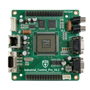
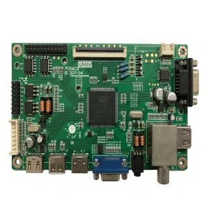
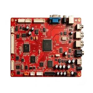
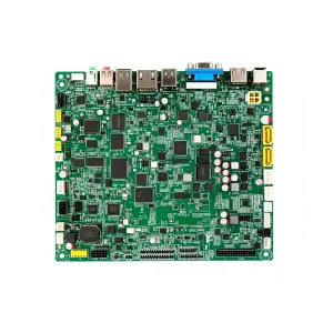
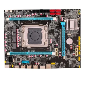
Explore our turnkey PCBA manufacturing capabilities across IoT, healthcare, power management, and human-machine interface assemblies.
The global printed circuit board manufacturing sector has reached a critical inflection point. As hardware architectures migrate toward multi-gigahertz digital signalling, ultra-fine-pitch ball grid arrays (0.35 mm pitch BGAs), and hybrid substrate rigid-flex topologies, the legacy reliance on disconnected 2D vector data introduces operational risk. Traditional Gerber RS-274D required manual aperture lists, leading to frequent optical misalignments and costly tooling iterations.
With modern Gerber RS-274X, apertures, coordinates, and polygon fills were integrated into single self-contained data packages. However, contemporary Tier-1 OEMs demand the advanced capabilities of Gerber X2 and Gerber X3, alongside open-standard IPC-2581 file structures. These modern vectors incorporate comprehensive machine-readable semantic data, stackup layer functions, drill attributes, and automated assembly fiducials directly into the manufacturing package.
A single coordinate rounding discrepancy in legacy Gerber files can alter annular ring clearance, causing micro-short circuits in internal copper layers or dry solder joints during convection reflow. Our Shenzhen engineering hub conducts 32 automated rules checks on every incoming Gerber archive.
By leveraging intelligent pattern recognition algorithms, STHL's CAM station contrasts client Gerber drill files against our laser direct imaging (LDI) compensations, eliminating manual aperture corrections and mitigating signal attenuation.
| PCB Data Standard | Aperture Definition | Layer & Stackup Mapping | Pick-and-Place Centroid | DFM Cycle Acceleration | Recommended Industrial Scope |
|---|---|---|---|---|---|
| Gerber RS-274D (Legacy) | External text list (manual) | Manual engineering assignment | Separate file required | Baseline (High risk of error) | Obsolete; legacy repair only |
| Gerber RS-274X (Standard) | Embedded vector definitions | Standard naming convention | Separate XY file required | +40% Efficiency | General Consumer & Industrial IoT |
| Gerber X2 / X3 | Fully integrated & indexed | Native layer functions & stackup | Embedded footprint & centroid (X3) | +75% Efficiency | Medical Devices, Automotive, Aerospace |
| IPC-2581 Consortia | XML-based holistic schema | Complete dielectric & netlist tree | Fully bidirectional automation | +85% Efficiency | High-Density High-Speed Server & Radar |
Navigating modern procurement requires more than low BOM cost—it demands robust risk diversification, rapid response to component allocations, and automated manufacturing execution.
Within a 30-kilometer radius of our Bao'an facility sits the highest concentration of raw laminate manufacturers (Shengyi, ITEQ, Rogers), copper foil suppliers, chemical plating houses, and franchised semiconductor distributors on earth.
This spatial density reduces material transit times from weeks to mere hours, safeguarding manufacturing schedules from international logistical bottlenecks.
Every bare board fabricated from client Gerber files is marked with a 2D matrix barcode. Our Manufacturing Execution System (MES) records solder paste inspection (SPI) heights, component reel lot numbers, reflow thermal profiles, and AOI optical captures.
If a field failure occurs years later, clients can trace down to the individual operator, placement feeder, and component batch within seconds.
Geopolitical trade restrictions and allocation cycles make global component sourcing precarious. STHL maintains direct vendor agreements with over 100 franchised global distributors (DigiKey, Mouser, Arrow, Avnet) and verified domestic foundries.
Our in-house incoming material laboratory deploys X-ray fluorescence (XRF) spectroscopy and decapsulation microscopy to verify silicon authenticity.
Evaluating total landed cost, engineering friction, and long-term qualification overhead in high-reliability PCB manufacturing.
Startups and enterprise R&D teams require rapid prototype spins (5 to 25 units) using production-grade SMT feeders without prohibitive setup surcharges, ensuring identical physical tolerances when transitioning to 100k+ mass runs.
Active lifecycle tracking is essential. Our 50+ engineering team flags End-of-Life (EOL) or active lead-time spikes early, recommending verified pin-compatible form-fit-function (FFF) alternative ICs to protect production continuity.
Rigorous contractual non-disclosure agreements (NDAs) enforced prior to Gerber or schematic extraction. Firmware hex code is loaded via air-gapped programming rigs with strict cryptographic key lifecycle disposal.
Operating bonded warehouse operations with integrated DHL, FedEx, and UPS priority dispatch. STHL maintains a consistent 99.5% on-time delivery rate across the US, Europe, East Asia, and Latin America.
Operational data from Shenzhen STHL Electronics Co., Ltd. — Building electronics hardware since 2006.
Our Quality Management Systems (QMS) undergo rigorous third-party surveillance audits, ensuring absolute compliance with international aerospace, automotive, medical, and environmental regulations.




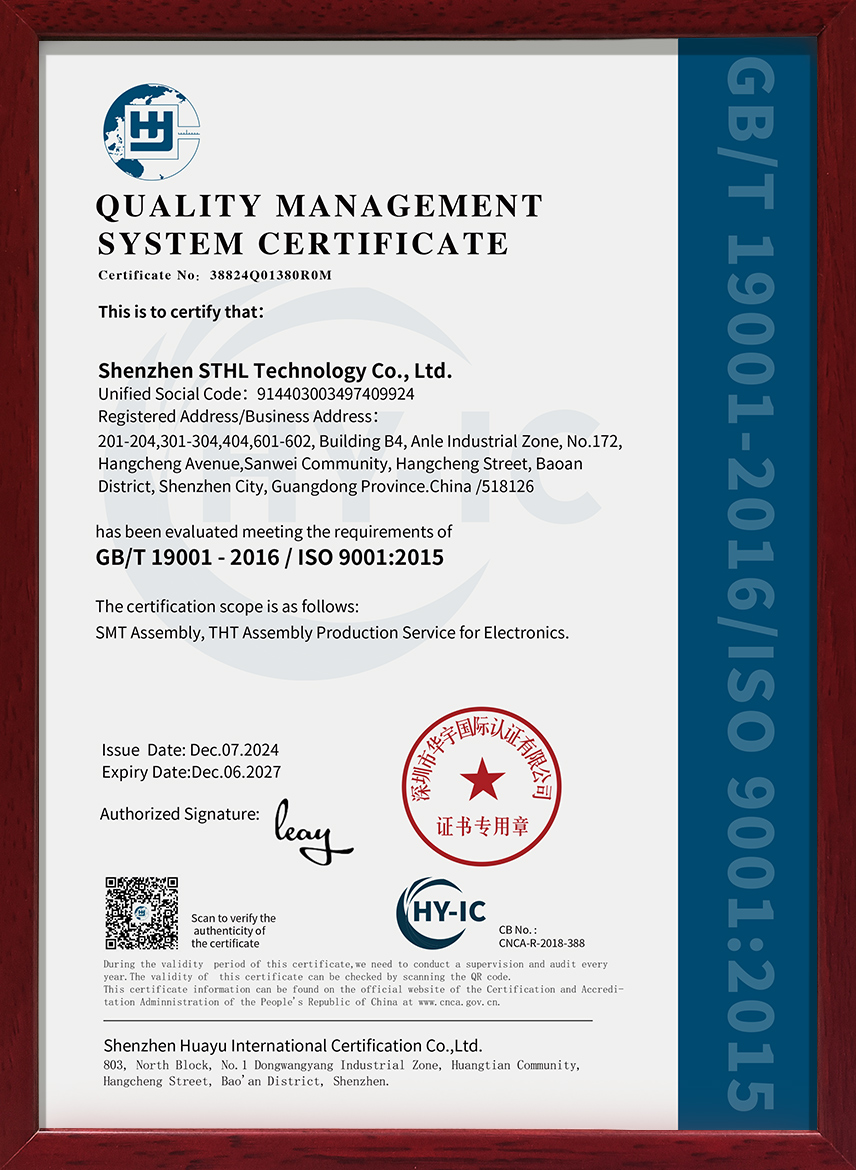
Governing bare PCB production, procurement, and SMT assembly lines.
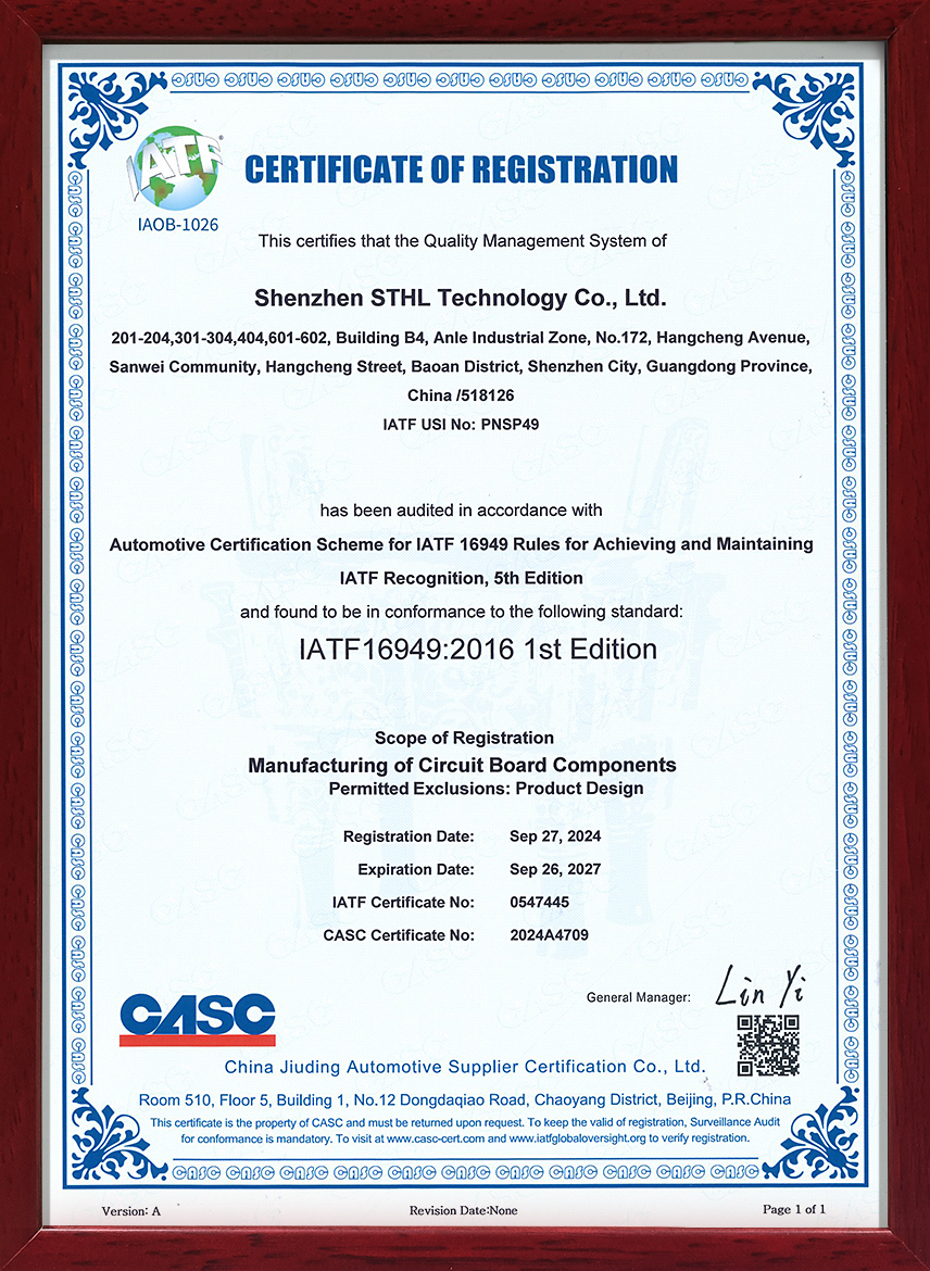
Specialized failure mode effects analysis (FMEA) for vehicle electronics.
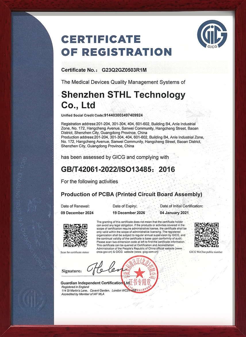
Full process validation and clean-room assembly for medical hardware.
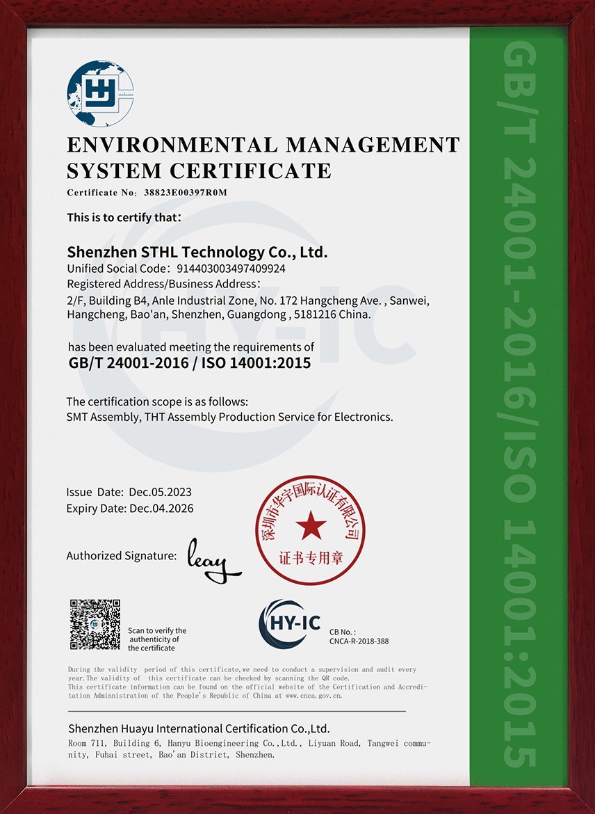
Systemic energy efficiency, lead-free soldering, and waste management.
A closed-loop manufacturing pipeline designed to capture design vulnerabilities before physical fabrication begins.
Receipt of RS-274X or Gerber X2 files under NDA. CAM engineers perform full Design Rule Checks (DRC) on track spacing, drill aspect ratios, and solder resist clearances.
Procurement cross-references client BOMs against franchised distribution inventories. Component authentication, lot-code logging, and dry-cabinet storage for moisture-sensitive devices.
Inner layer etching, automated optical inspection (AOI) before lamination, laser direct imaging (LDI), and automated optical registration for multi-layer via alignment.
3D Solder Paste Inspection ensures aperture deposition uniformity. High-speed Yamaha pick-and-place placement followed by 10-zone nitrogen reflow oven profile verification.
Hidden solder joints on BGA and QFN packages verified via 3D computed tomography X-Ray. In-Circuit Testing (ICT) and custom Functional Testing (FCT) jigs run at full clock speed.
Ultrasonic welding, conformal robotic spray coating, cable harness integration, enclosure assembly, and custom ESD export crating with real-time customs dispatch tracking.
We work seamlessly with Fortune 500 tech leaders, dynamic industrial OEMs, and tier-1 semiconductor foundries worldwide.












Unfiltered evaluations from engineering teams in North America, Europe, Oceania, and Latin America.
"Excellent team to work with and fast delivery with high-quality boards. We are very happy to work with such a good supplier. Thanks again."

"Please extend my thanks to your team for the hard work in preparing these samples. This experience has strengthened my confidence in your company, and I look forward to discussing bulk orders soon."

"We are satisfied with the last order. You did a great job on those boards and the lead time was short. I will place a new order soon."

"The order was perfect—exactly as specified, with top quality. Highly recommend this reliable supplier."

"Very fast delivery, professional supplier and professional product. We will place a new order very soon!"

"We have tested all the boards and I am highly pleased. I will repeat my order soon. Thank you again for your excellent service."

Comprehensive technical guidance compiled by senior CAM specialists and procurement directors.
To provide an immutable DFM report and price quotation, we request: 1) Complete Gerber files in RS-274X, Gerber X2, or IPC-2581 format (including all copper, solder mask, silkscreen, paste, and drill NC Excellon layers); 2) A comprehensive Bill of Materials (BOM) in Excel with manufacturer part numbers (MPN), approved alternate second sources, reference designators, and quantities; 3) Centroid (Pick-and-Place X-Y coordinate) file with component angle rotations; and 4) Detailed acceptance specifications indicating test procedures and conformal coating boundaries.
Prior to launching any bare-board production, our engineering desk outputs a comprehensive DFM/DFA engineering query (EQ) document. We check for minimum copper trace width/spacing (down to 3.0 mil / 3.0 mil on HDI), drill-to-copper clearances, isolated copper stubs that could cause antenna signal degradation, and insufficient solder dam widths (minimum 4.0 mil) to prevent bridge shorts during surface mount convection reflow. Production only commences after customer written sign-off on the generated CAM stackup drawing.
Yes. Our high-precision Yamaha SMT lines feature optical alignment systems capable of placing down to 01005 (0402 metric) passives and micro-BGA packages with ball pitches as fine as 0.30mm with ±0.03mm placement accuracy. Laser direct-etched electro-polished stencils paired with 3D Solder Paste Inspection (SPI) ensure volume and height tolerances within ±10% across every pad.
We operate strict physical and cyber IP governance protocols. We execute bilateral Non-Disclosure Agreements governed under recognized international jurisdiction before accepting any technical collateral. Firmware flashing is handled through segmented internal networks with zero internet breakout, using automated IC programmers that log serial counts to prevent over-flashing or unauthorized binaries proliferation.
For standard 2-to-8 layer rigid FR-4 prototypes, bare board fabrication can be expedited to 24 to 48 hours. When combined with our turnkey component procurement and quick-turn SMT scheduling, assembled prototypes typically ship in 5 to 7 working days. Standard volume runs (1,000 to 100,000+ units) follow a predictable 15 to 20 working day turnaround, subject to active semiconductor lead-time parameters.
Yes. Beyond electrical flying probe and bed-of-nails In-Circuit Testing (ICT), our 50+ engineering team builds bespoke Functional Testing (FCT) jigs with automated pneumatic fixtures, digital signal generators, oscilloscope integration, and RF spectrum analysis. We also provide complete electro-mechanical box-build assembly, including custom CNC or injection-molded enclosures, display optical bonding, wiring harnesses, and final consumer packaging.
Turnkey electronic assemblies manufactured to IPC-A-610 Class 2 & Class 3 industrial criteria.


Send your RS-274X, Gerber X2, or IPC-2581 archive along with your BOM. Our senior CAM engineers deliver an actionable DFM review within 24 hours under full NDA.
