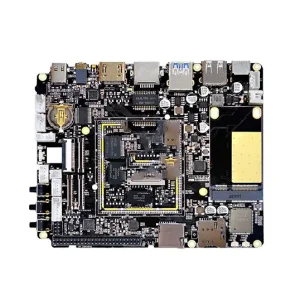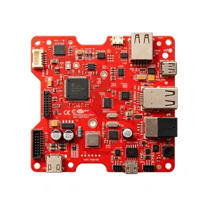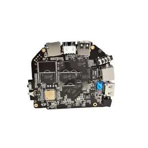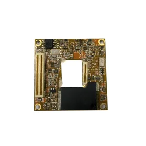
Pre-engineered turnkey assemblies calibrated for USA industrial environments, automotive standards, and communications infrastructure.
Modern OEMs in the United States operate under demanding market windows, strict Federal regulatory landscapes, and severe unit-cost pressures.
While domestic PCB fabrication within the US excels in immediate Class 3 quick-turn prototyping, mass commercial scaling often stumbles against labor constraints, elevated tooling expenditures, and narrow substrate access. Conversely, partnering directly with offshore facilities frequently carries liabilities involving intellectual property integrity, time-zone disconnects, and volatile supply chain visibility.
The STHL hybrid delivery framework resolves this dichotomy. By harmonizing western-standard DFM validations and engineering accountability with our 10,000+ m² smart factory infrastructure in Shenzhen, American enterprises secure unmatched cost structures without conceding IPC-A-610 Class 3 workmanship, ITAR alignments, or component authenticity.
| Metric Attribute | Standard US Domestic | STHL Hybrid Solution |
|---|---|---|
| Mass Volume Unit Cost | Elevated (3-5x Baseline) | Highly Optimized / Factory-Direct |
| Component Availability | Subject to Local Rep Quotas | 500k+ Active Parts, 100+ Factory Channels |
| Rapid Prototyping | 3-5 Working Days | 48-Hour Fast-Track Build & Express Air |
| Quality System | ISO 9001 Typical | IATF 16949 / ISO 13485 / IPC-A-610 Class 3 |
| High-Layer HDI Scalability | High Tooling Fees | Zero NRE Upcharges on Scheduled Volumes |
Providing deterministic electronic hardware architectures engineered to exceed harsh operating conditions across the United States industrial spectrum.
Automotive tiers demand relentless endurance under mechanical vibration and thermal oscillation. Engineered strictly under IATF 16949 standards, our PCBA solutions drive advanced battery management systems (BMS), On-Board Chargers (OBC), and in-vehicle communication modules, surviving ambient extremes from Alaska to the Mojave Desert.
Compliant with FDA QSR and ISO 13485 mandates, our clean-room assembly lines support critical patient telemetry, ECG cardiac monitors, and non-invasive surgical navigation hardware. We implement 100% AOI, functional in-circuit profiling, and device master record (DMR) retention ensuring full legal and clinical defensibility.
Decarbonization projects across the North American grid demand ruggedized converters and wind power controllers. We deploy heavy copper layers up to 6oz, specialized thermal vias, and thick conformal coatings (polyurethane/silicone) to prevent dendritic growth and ionic contamination in remote field installations.
Providing high-density interconnect (HDI) multilayers, flex, and rigid-flex circuits for factory robotics, smart sensor clusters, and precision drilling control apparatus. Fully traceable component sourcing guarantees immunity against counterfeit silicon across extensive lifecycles.
Situated in the heart of Shenzhen’s Bao'an electronics cluster, STHL combines massive component proximity with ultra-modern surface-mount technology lines.
Global chip shortages demonstrated that procurement agility determines product survival.
Traditional American assembly houses often source exclusively through Tier-1 catalog distributors with rigid allocation structures. STHL leverages direct direct-factory alliances with primary semiconductor fabs and franchised regional aggregators (Arrow, Avnet, DigiKey, Mouser, Verical), unlocking over 500,000 active references with zero middlemen markups.
Our certified counterfeit avoidance laboratories perform de-capsulation testing, solderability assessment, and optical microscope verification before any batch reaches the feeder carriage. This enables our American OEM clients to maintain aggressive product delivery schedules, circumvent component obsolescence, and systematically reduce Bill of Materials (BOM) overhead by 20% to 40%.
Anticipating next-decade signal velocities, complex thermal dynamics, and extreme miniaturization across critical global applications.
Scaling to 25μm trace/space configurations and stacked microvia geometries enabling complex BGA pitches down to 0.35mm. Ideal for advanced AI-accelerator edge processors, compact computing modules, and ultra-miniaturized body-worn telemetry nodes.
Processing Rogers, Taconic, and Teflon PTFE composite substrates engineered for low dielectric loss (Df < 0.002) at 77GHz radar and Sub-6GHz telecommunications bands, delivering flawless phase integrity and controlled differential impedance tolerances within ±5%.
Integrating heavy-copper internal planes (up to 12oz) paired with aluminum/copper core IMS systems achieving thermal conductivity levels above 3.0 W/m·K. Vital for automotive battery inversion circuitry and high-lumen commercial lighting drivers.
Deploying algorithmic deep-learning models across 3D Solder Paste Inspection (SPI) and automated multi-angle X-ray examination (AXI), isolating micro-voiding inside bottom-terminated components (QFN/BGA) below 10% volume thresholds automatically.
Transparent operational clarifications for United States procurement directors, supply chain managers, and hardware engineering leaders.
Continuous production-proven assemblies engineered for heavy equipment, automotive safety, and specialized sensory systems.