Engineered for extreme environmental compliance, high vibrational resilience, and continuous cycle execution across automotive, industrial edge, and smart grid applications.

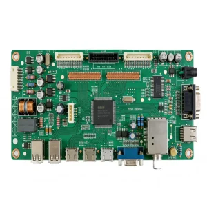
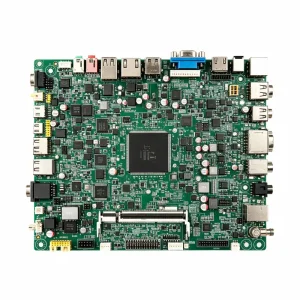

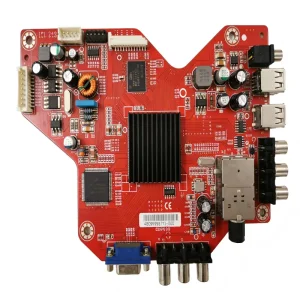
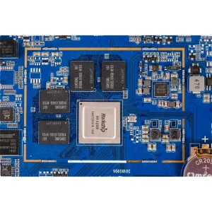

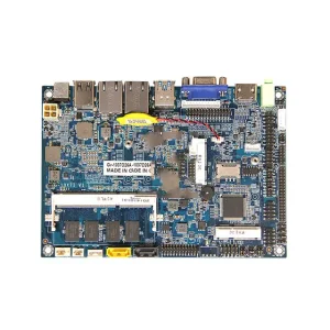
In an era marked by rapid obsolescence, dynamic tariff regimes, and micro-pitch silicon packages, tier-1 OEMs require an EMS factory that acts as an agile extension of their core engineering department.
Global procurement teams cannot afford single-point failures. Through STHL's direct relationship with authorized global distributors (Mouser, Digi-Key, Avnet, Arrow) and over 100+ vetted domestic silicon vendors, we mitigate component obsolescence through early BOM health checks and verified pin-compatible form-fit-function (FFF) second sources.
Whether navigating RoHS 3, REACH, Conflict Minerals, or UL 94V-0 fire retardancy ratings, enterprise buyers require full material lineage. Every batch fabricated within our Shenzhen facility is backed by cloud-synchronized ERP/MES lot codes, linking bare PCB prepregs, solder chemistry lots, and active IC wafers directly to final assembly bar codes.
Procuring in China is no longer merely about low labor costs; it is an architectural advantage. By consolidating PCB panel layout optimization, automated high-density SMT mounting, in-house tooling creation, functional test fixture (FCT) fabrication, and complete box-build integration under one roof, our clients reduce shipping loops and tariffs by up to 28%.
STHL delivers comprehensive turnkey manufacturing ecosystems specifically tailored for high-complexity electronics sectors where field downtime is unacceptable.
Certified workflows for Battery Management Systems (BMS), EV charging control boards, and in-cabin infotainment. We execute high-reliability thick-copper routing, heavy-duty wave soldering, and automated thermal paste dispensing to safely handle high transient currents and automotive temperature ratings (-40°C to +125°C).
Manufactured strictly within ISO 13485 clean-room environments. We maintain ultra-low contamination control, automated selective conformal coating against physiological liquids, 100% 3D X-ray inspection for void-free BGA balls, and micro-fine pitch surface mounting for sensitive patient diagnostic sensors.
High-reliability assemblies engineered to conquer micro-vibrations, extreme thermal cycling, and cosmic radiation. Utilizing IPC-A-610 Class 3 assembly protocols, high-Tg Rogers or polyimide laminates, and nitrogen reflow ovens to guarantee zero intermetallic embrittlement.
Tailored for long deployment lifecycles (10–15+ years). Featuring embedded PLC bus interfaces, heavy-current busbar soldering, specialized potting encapsulation, and functional environmental stress screening (ESS) to guard against electromagnetic interference and high humidity.
Operating 10,000+ m² of automated surface-mount lines, through-hole insertion cells, and cleanroom test environments powered by industry-leading equipment.
As semiconductor designs scale downward to smaller geometries and silicon photonics emerge, our manufacturing lines continually upgrade to stay ahead of next-generation packaging demands.
Full deployment of 12M-pixel high-speed optical inspection, Koh Young 3D solder paste inspection (SPI), and closed-loop feedback controlling squeegee pressure and alignment offsets in real time.
Expansion of any-layer HDI capabilities, cavity PCB micro-milling, and embedding passive/active components within internal substrate cores to shorten signal transit paths for 5G mmWave equipment.
Machine learning-powered thermal profile modeling that correlates ambient humidity, board copper distribution, and individual component mass to establish individualized solder profiles with zero defect risk.
Integration of low-temperature soldering (LTS) alloys reducing thermal stress by 40%, paired with zero-effluent clean chemical rinse systems and bio-degradable conformal masking chemistries.
Eliminating the perceived risks of offshore manufacturing through stringent institutional protections, bilateral NDAs, and door-to-door Incoterms execution.
Intellectual property is your company's greatest asset. We execute mutually enforceable Non-Disclosure Agreements before your Gerber data, schematics, or firmware binaries are loaded to our internal engineering servers. Encrypted access and isolated programming stations ensure absolute software integrity.
Cross-border customs and brokerage clearances can quickly become bottlenecks. STHL coordinates direct multimodal air and ocean freight (DAP/DDP) covering port handling, import documentation, and local logistics directly to warehouses in North America, the European Union, Australia, and APAC.
Misunderstandings during engineering inquiries delay product launches. Every project at STHL is paired with an IPC-certified bilingual applications engineer who translates your design intent into clear design-for-manufacturability (DFM) and design-for-test (DFT) optimization reports within 24 hours.
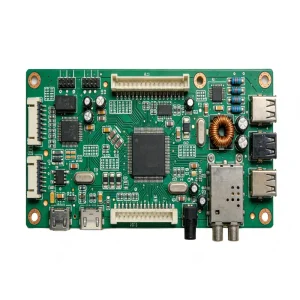
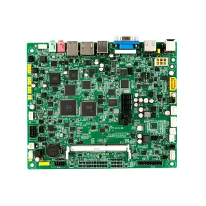
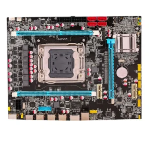
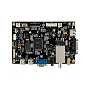
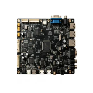
Explore our demonstrated field applications across industrial IoT telemetry, flight avionics instrumentation, and high-frequency power electronics.


Clear, direct answers regarding fabrication limits, component procurement governance, testing protocols, and volume ramp timelines.
