In the contemporary landscape of high-speed digital communications, mission-critical automotive subsystems, and ultra-compact medical diagnostics, the margin for hardware iteration error is virtually non-existent. Prototyping is no longer merely a validation phase—it is an algorithmic stress test of supply chain resilience, bare-board manufacturability, and thermomechanical integrity.
Iterative algorithmic checking of Gerber and IPC-2581 databases eliminates copper slivers, unintended acid traps, aspect ratio mismatches, and component solder-shadowing prior to bare-board panelization, shaving weeks off the commercialization cycle.
Direct API synchronization with global authorized distribution hubs safeguards bills of materials against counterfeit silicon, grey-market passives, and moisture-compromised MSL packages, ensuring baseline functional authenticity.
Prototyping boards on high-precision SMT lines identically configured for medium-to-mass production yields uncompromised baseline reflow profiles, thermal gradients, and wave parameters that carry directly into full manufacturing scale.
Hardware teams frequently fall into the trap of using localized low-capability quick-turn vendors that skip IPC Class 3 plating standards or rely on non-automated manual soldering. When the transition to automated mass production occurs, issues such as tombstoning, micro-voiding under bottom-terminated components (QFN/BGA), and uncontrolled impedance drift disrupt deliveries. China's premier cluster bridges this gap by enforcing production-grade industrial equipment directly onto the rapid prototype board phase.
Despite recent discussions around nearshoring and regional manufacturing reshoring across Europe and North America, the Pearl River Delta (Shenzhen-Dongguan-Huizhou) commands unprecedented velocity due to its physical co-location of substrate copper laminators, chemical suppliers, precision tooling houses, and global passive components repositories.
Raw substrates (FR-4 High-Tg, Rogers, Polyimide, Aluminum core) are sourced in hours rather than weeks. Rapid turnaround of multi-layer quick-turn boards (24-48 hours for 4 to 8 layers) allows rapid iteration across hardware development sprints.
Eliminate multiple markups from middle-tier brokerages. Engaging directly with certified Chinese EMS manufacturing facilities lowers prototype expenditure while preserving seamless scalability to high-volume assembly.
STHL partners directly with Arrow, Avnet, Digi-Key, Mouser, and verified regional franchised distributors. Every reel and tray enters cleanrooms governed by barcoded MES entry systems, ensuring absolute component authenticity.
From micro-vias in High-Density Interconnect (HDI) structures to controlled thermal expansion in metal-backed power electronics, our manufacturing facilities adhere to strict IPC Class 2 and Class 3 manufacturing parameters.
| Process Parameter | Standard Prototype Capability | Advanced / High-Precision Capability |
|---|---|---|
| Layer Count Range | 1 - 8 Layers (FR4, CEM-1, Aluminum) | Up to 48 Layers (HDI, Rigid-Flex, Anylayer) |
| Min. Trace Width / Spacing | 3.5 mil / 3.5 mil (0.089 mm) | 2.0 mil / 2.0 mil (0.050 mm) for HDI micro-routing |
| Min. Mechanical Drill Hole | 0.20 mm (8 mil) | 0.15 mm (6 mil) |
| Laser Micro-Via Diameter | 0.10 mm (4 mil) | 0.075 mm (3 mil) UV Laser Drilled |
| Controlled Impedance Tolerance | ± 10% standard | ± 5% with TDR polar validation coupon |
| Surface Finishes Available | HASL lead-free, ENIG (Electroless Nickel) | ENEPIG, Immersion Silver/Tin, Hard Gold Plating |
| SMT Component Placement | 0402 passives, 0.5 mm pitch QFP/BGA | 01005 passives, 0.3 mm ultra-fine pitch micro-BGA, PoP |
| Automated Solder Inspection | 2D AOI Inline, Offline Sample X-Ray | Inline 3D SPI + 3D AOI + AXI (3D Computed Tomography) |
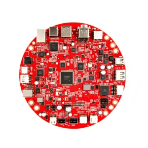
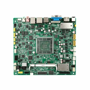
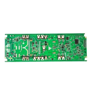
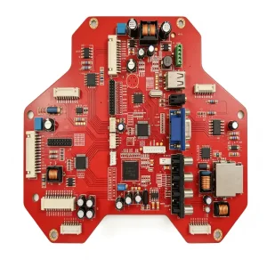
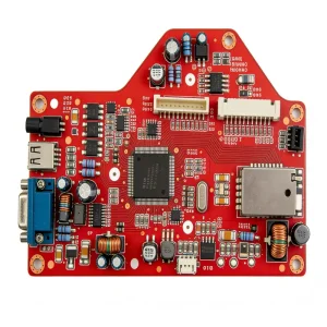
Explore our manufactured assemblies across gas sensing, imaging, high-reliability aerospace, and power conversion applications.

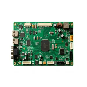
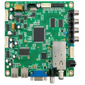
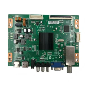

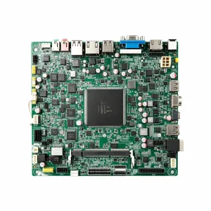
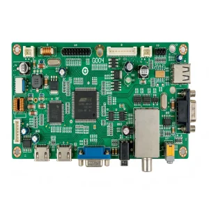
A look at the 7-stage quality gating protocol operating across our Bao'an facility. Every single bare board and assembled circuit is bound to an ERP work order, with component reel lot-level records preserved for 10 years.
Automated validation against 800+ design rules covering drill-to-copper clearances, solder mask dam integrity, annular ring adequacy, and thermal relief configurations for enhanced reflow yields.
Koh Young 3D SPI platforms analyze solder paste deposition height, volume, area, and bridging before components reach pick-and-place nozzles, preventing 70% of potential assembly anomalies.
Multi-angle 3D AOI measures component coplanarity and fillet height, while high-resolution X-Ray Inspection detects BGA head-in-pillow, package voids, and barrel fill on through-hole pins.
Dual-shuttle flying probe systems verify passive values, diode polarity, and detect micro-shorts on dense prototype boards without the non-recurring engineering expense of custom bed-of-nails fixtures.
Custom-built modular jigs simulate live operational voltage, CAN bus/Ethernet packet throughput, RF power attenuation, and sensor calibration curves under programmed MCU firmware routines.
Automated selective conformal coating (polyurethane, acrylic, silicone) followed by thermal cycling chambers (-40°C to +125°C) to purge latent component infant mortality prior to shipment.
A prototype board is fundamentally deficient if it cannot pass target market compliance. STHL maintains an active portfolio of audited certifications guaranteeing compliance with medical, automotive, aerospace, and industrial criteria.
Automotive quality management system requiring rigorous APQP (Advanced Product Quality Planning), PPAP (Production Part Approval Process), and zero-defect statistical process controls for in-cabin and powertrain electronics.
Medical device quality assurance with documented component lineage, cleanroom handling protocol, and strict risk assessment protocols for Class I, II, and III device sub-assemblies.
High-reliability electronics criteria for aerospace, mission-critical industrial, and defense hardware where uninterrupted continuous performance is paramount.
Environmentally safe manufacturing enforcing strict limits on lead, cadmium, mercury, polybrominated biphenyls, and SVHCs (Substances of Very High Concern) under EU Directives.
Demonstrating how rapid PCB prototyping translates into industrial field reliability across diverse physical and operational environments.
Heavy-copper circuits (3 oz to 6 oz) integrated with thick ceramic thermal pads handle continuous 400V/800V DC pack discharge rates. Isolation barrier clearances prevent arching under extreme vibration.
Intrinsically safe circuit designs featuring current-limiting Zener barriers, encapsulated potting modules, and high-temp FR-4 (Tg 180°C) for harsh petrochemical and subterranean deployment.
Polyimide-based rigid-flex multilayer assemblies eliminating heavy internal wiring harnesses, tested under MIL-STD-810 thermal shock profiles and micro-sectioned for inter-plane via barrel thickness.
As computing edge nodes migrate toward AI tensor acceleration, PCB prototype manufacturing must adapt to high-frequency dielectric materials, embedded passives, and advanced thermal dissipation substrates.
Deep learning vision algorithms scan Gerber layers in real-time, autonomously predicting thermal warpage risks during reflow and recommending optimal component package orientations.
Cost-effective hybrid stack-ups fusing standard FR-4 prepreg cores with high-frequency hydrocarbon ceramics (e.g., Rogers RO4350B) to deliver 77 GHz radar performance within modest budgets.
Routing capacitors and resistors directly inside internal laminate dielectric cavities, freeing surface area for ultra-dense System-in-Package (SiP) and BGA footprints.
Clear, direct answers regarding engineering files, delivery lead times, IP protection, and assembly standards.
To deliver an exhaustive engineering audit and quote within 24 hours, we require: (1) RS-274X Gerber or ODB++ fabrication data, (2) Detailed Bill of Materials (BOM) containing manufacturer part numbers (MPN), reference designators, and approved alternative vendors, (3) Centroid Pick-and-Place (XY coordinates and rotation angle), and (4) Assembly drawings outlining conformal coating boundaries, programming instructions, or functional test requirements.
We execute legally binding bilateral Non-Disclosure Agreements (NDAs) prior to receiving any design files. Internally, production data is compartmentalized through encrypted intranet servers, preventing engineering schematics from being copied to external storage devices. Firmware flashing is conducted using encrypted binary programming algorithms inside isolated, video-monitored cleanrooms.
Yes. All prototype boards are fabricated using the same high-tier production machinery (Yamaha and Fuji SMT lines, Heller reflow ovens, and Koh Young 3D inspection) utilized for volume runs. The thermal reflow profiles, wave solder parameters, stencil apertures, and MES traceability codes developed during the prototype phase transition directly into mass manufacturing, eliminating re-engineering risks.
Our dedicated procurement engineering team actively cross-references pin-compatible drop-in replacements using internal component databases. Before any substitution is implemented, our hardware team submits full parametric comparison sheets and datasheet comparisons for client approval, ensuring identical voltage thresholds, clock rates, and thermal margins.
Standard quick-turn bare PCB prototypes (2 to 6 layers) can be manufactured in 24 to 48 hours. Turnkey PCBA assembly typically requires 5 to 7 business days from component arrival. For expedited NPI cycles, dedicated fast-track procurement options reduce end-to-end delivery times to under 10 business days worldwide.
Review our specialized assemblies for charging systems, high-efficiency power supplies, physiological medical instruments, and camera modules.