Engineered in our dust-free Shenzhen smart factory with 7 high-speed SMT lines and zero minimum order quantity (MOQ).
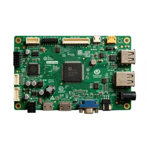
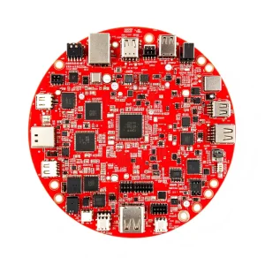
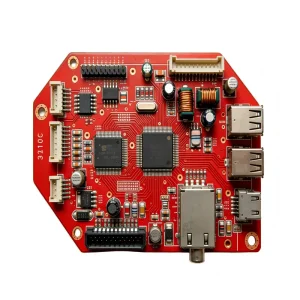
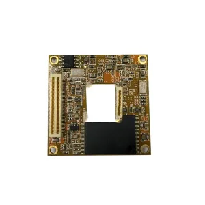

In the contemporary electronics engineering paradigm, time-to-market is the primary determinant of commercial survival. Rapid PCB prototyping has evolved from an ad-hoc laboratory validation process into a mission-critical phase of modern Agile Hardware Development.
Across North America, the European Union, Japan, and Southeast Asia, original equipment manufacturers (OEMs) and disruptive IoT innovators are undergoing unprecedented compressions in product life cycles. The transition toward high-density computing, generative AI micro-controllers, edge inference architectures, and electrification demands hardware validation turnarounds within days rather than months. Historically, a failure in early-stage board fabrication could derail commercial launch windows, creating multi-million-dollar opportunity costs. As a consequence, hardware procurement leaders are actively reconfiguring their prototyping workflows, turning away from fragmented, multi-vendor models toward vertically integrated EMS partners capable of executing PCB fabrication, precision component procurement, and Surface Mount Technology (SMT) assembly in a singular, closed-loop environment.
Prototyping serves not merely to confirm schematics and netlists, but to rigorously de-risk Design for Manufacturability (DFM), Design for Assembly (DFA), and Design for Testability (DFT). High-speed signal integrity, thermal dissipation balance, fine-pitch Ball Grid Array (BGA) coplanarity, and solder joint reliability under mechanical stress must be validated in early prototype spins. Failing to detect layer misalignments, impedance mismatches, or component pad design flaws at the pilot stage inevitably yields catastrophic yields during mass scale-up. Consequently, high-capability Chinese PCB prototype manufacturers have become the premier anchor for worldwide hardware innovators seeking rapid verification without compromising aerospace, automotive, or medical quality thresholds.
Accelerating from Gerber sign-off to functional assembly within 24 to 72 hours. Hardware engineering sprints now mirror software release cadences, enabling multiple physical iterations per quarter.
Prototypes routinely integrate 01005 passives, 0.35mm pitch BGAs, and blind/buried microvias via Laser Direct Imaging (LDI), demanding extreme precision long before production ramp-up.
Executing pilot runs on the identical high-precision SMT lines (Yamaha, Panasonic, Fuji) destined for high-volume execution, eliminating line-tuning discrepancies and yield surprises.
Shenzhen’s Bao’an and Pearl River Delta manufacturing ecosystem represents the world's most concentrated cluster for electronic design, bare-board lamination, component logistics, and automated assembly.
The decisive competitive edge of China’s PCB prototyping sector does not rely solely on unit economics; it is rooted in unrivaled supply chain density and cross-disciplinary infrastructure. Within a 30-kilometer radius in Shenzhen, an engineering team can procure specialized copper clad laminates (FR-4, Rogers, Megtron 6, Polyimide), custom laser-cut electropolished step-up stencils, standard active silicon from international franchised distributors (Arrow, Avnet, Digi-Key, Mouser), and rare domestic passives within mere hours. What requires three weeks of procurement logistics in North America or Western Europe is executed in Shenzhen within half a working shift.
Shenzhen STHL Electronics leverages this hyper-concentrated infrastructure from its 10,000+ m² facility in Bao'an. Running 7 automated SMT lines equipped with 3D Solder Paste Inspection (SPI), multi-axis Automated Optical Inspection (AOI), and high-resolution Transmission X-Ray Inspection, prototype assemblies achieve mass-production caliber solder joint integrity. Furthermore, Chinese manufacturers have pioneered automated digital quoting, ERP-integrated Gerber parsing algorithms, and dynamic pick-and-place programming, which compress pre-production engineering lead times from days to a matter of minutes.
Direct electronic data interchange (EDI) links with 100+ global and regional distributors allow immediate component kitting, neutralizing supply bottlenecks.
Dedicated in-house laser stencil fabrication and CNC fixturing eliminate external hand-offs, enabling prototype paste printing within 4 hours of design lock.
Compliance with IPC-A-610 Class 2/3, IATF 16949 automotive defect prevention, ISO 13485 medical device systems, and ISO 9001 certified governance.
Overhead efficiencies translated into competitive pilot costs without sacrificing equipment caliber, freeing client capital for software and core R&D.
Prototyping requirements diverge drastically across industrial, medical, and aerospace domains. A generic consumer board cannot withstand the vibration, thermal cycling, and dielectric scrutiny demanded by safety-critical electronics.
| Vertical Domain | Critical Board Specifications | Assembly & Metallurgy Norms | Mandatory Verification Protocols |
|---|---|---|---|
| Aerospace & Avionics (e.g., Flight Computers, Cockpit Voice Recorders) | Polyimide / High-Tg FR-4, Blind/Buried Vias, Controlled Impedance ±5%, Heavy Copper | IPC-A-610 Class 3, ENIG/HASL Lead-Free, Underfill on large BGAs, Conformal Coating | 3D X-Ray Voiding <10%, Boundary Scan, Thermal Shock (-55°C to +125°C), Random Vibration |
| Automotive Electronics (e.g., TCU, OBC, Battery Management) | Ceramic, Aluminum IMS, Halogen-Free High-Tg (>170°C), Thick Copper (3oz-6oz) | IATF 16949 Audited Lines, SAC305 Solder Alloy, Automated Selective Soldering for Connectors | In-Circuit Testing (ICT), Automated Optical Inspection, Moisture Sensitivity Pre-baking |
| Medical & Implantable (e.g., Pacemakers, Diagnostic Scanners) | Ultra-thin Rigid-Flex, Roger High-Frequency Laminates, Sub-0.1mm Trace/Space | ISO 13485 Controlled Workcell, Biocompatible flux residues, Cleanroom assembly | 100% Flying Probe Testing, Full Component Lot Serial Traceability, Functional Firmware Validation |
| Industrial Automation (e.g., Electric Cranes, Solar Monitoring) | Multi-layer FR-4, Heavy Copper Traces, Galvanic Isolation Barriers, Surge Gaps | IPC Class 2, Wave Soldering for high-current terminal blocks, Silicone Potting support | Hi-Pot Dielectric Voltage Withstand, Burn-in Life Cycle Chamber Testing, AOI verification |
Integrating flexible polyimide inner cores with rigid external outer FR-4 layers. Ideal for wearables, aerospace avionics, and space-constrained medical instrumentation where weight and dynamic flexing cannot be compromised.
Aluminum and copper base insulated metal substrates (IMS) developed specifically for high-power LED arrays, electric vehicle on-board chargers (OBC), and photovoltaic solar inverter controllers requiring rapid heat dissipation.
Precision hybrid multi-layer stack-ups combining Rogers RO4350B or Taconic with standard FR-4 prepregs, delivering tight dielectric constant (Dk) tolerance and ultra-low dissipation factor (Df) for 5G, VoIP, and radar equipment.
The confluence of artificial intelligence hardware, edge computing, environmental directives, and advanced packaging is fundamentally reshaping China’s electronics manufacturing landscape.
Transitioning from traditional subtractive etching toward modified Semi-Additive Processes (mSAP). This unlocks 25µm/25µm trace width and spacing, essential for edge-AI neural accelerators and system-in-package (SiP) prototypes.
Machine learning algorithms now analyze incoming Gerber and ODB++ archives in real time, automatically flagging acid traps, starved thermal reliefs, insufficient annular rings, and solder bridge risks within seconds.
To safeguard warpage-sensitive ultra-thin packages and reduce carbon footprint, bismuth-tin (BiSn) and modified resin solder formulations are deployed, allowing reflow peaks below 180°C.
Zero-discharge wastewater recycling facilities and halogen-free base materials meet stringent European Union WEEE and RoHS directives, positioning prototypes for friction-free worldwide customs clearance.
Procuring PCB prototypes offshore requires clear protocols for data security, component pedigree, and schedule accountability. Global hardware buyers must balance cost efficiency with total project transparency.
A primary friction point for international engineering directors engaging Chinese manufacturers is the preservation of proprietary Intellectual Property (IP). Sophisticated EMS providers like STHL operate under stringent confidentiality ecosystems. Prior to receiving Gerber files, schematic diagrams, or proprietary firmware binaries, legally binding Non-Disclosure Agreements (NDAs) subject to designated international legal jurisdictions are executed. Internally, enterprise rights management (ERM) software restricts engineering file access exclusively to assigned project teams, while air-gapped programming stations safeguard proprietary HEX/BIN code during on-board flash deployment.
Equally critical is safeguarding against counterfeit electronic components. The gray market for active integrated circuits can introduce recycled, re-marked, or substandard silicon that causes phantom intermittent failures in field deployments. A certified China prototype manufacturer maintains direct authorized distribution agreements with primary semiconductor sources. Every reel, tube, and tray is subjected to incoming material inspection, including barcode traceability, anti-counterfeit microscopic marking inspection, solderability testing, and dry cabinet moisture barrier bag (MBB) handling per IPC/JEDEC J-STD-033 standards.
Firmware programming occurs within secure, audited workstations with restricted external network connections, preventing source code exposure or clone vulnerability.
Lot-level traceability linked to manufacturer Certificate of Conformance (CoC), allowing buyers to trace every integrated circuit back to the specific wafer foundry run.
Direct daily air cargo out of Shenzhen and Hong Kong international hubs delivers finished prototypes to European and North American facilities within 2 to 4 working days.
Engineered to exacting tolerances for energy systems, automotive control units, avionics, and high-speed multimedia peripherals.
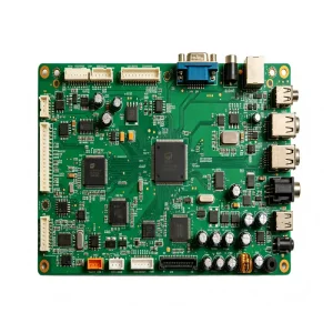

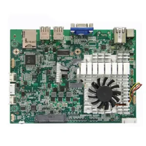
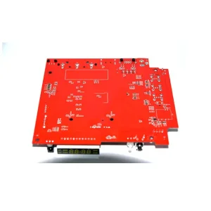

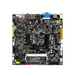
Detailed technical answers to common queries regarding DFM feedback, quick-turn lead times, testing coverage, and quality compliance for custom PCB prototypes.
