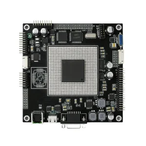
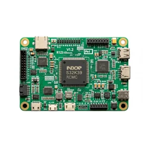
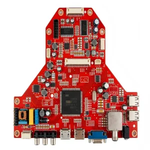
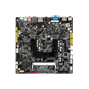
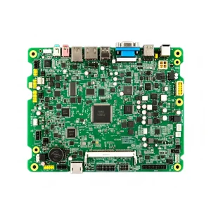
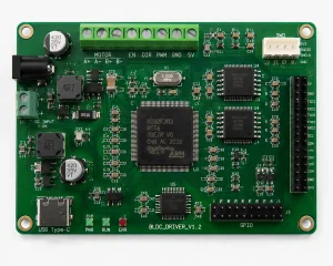
Direct from our dust-free SMT production lines: Mission-critical hardware engineering for industrial, automotive, and medical validation.
Understanding why leading technology innovators partner with specialized Chinese electronics manufacturing facilities to eliminate iteration latency and accelerate product time-to-market.
The global electronics hardware landscape has entered an era of rapid design iteration. Across artificial intelligence clusters, autonomous mobility, wearable medtech, and high-frequency edge IoT devices, hardware engineers no longer face leisurely design-and-test schedules. The traditional paradigm—where multi-week board turns separated architectural schematic freeze from experimental bench-testing—is wholly incompatible with modern commercialization pressures. As global research and development expenditure shifts heavily toward compressed NPI (New Product Introduction) cycles, the role of a capable China PCB Prototyping Factory has evolved from simple contractual fabrication into an indispensable engineering partnership.
Shenzhen, China, serves as the epicentre of this rapid hardware synthesis. The geographic proximity of bare-board raw materials, immediate availability of active silicon from authorized franchised distribution hubs, and native assembly infrastructure eliminate weeks of international transit overhead. Where European or North American local prototypes frequently incur four-to-six-week component lead times and cost-prohibitive low-volume fees, specialized Chinese prototyping facilities operate around clockwork 24-to-72 hour fabrication and assembly loops. This agility empowers global hardware startups and Fortune 500 tier-1 enterprises alike to iterate physical schematics, validate thermals, and calibrate high-speed signal integrity at fractional cycle costs.
Over 80% of the world’s component supply and specialized chemical substrate fabrication reside within a 50-mile radius in the Greater Bay Area, mitigating overseas transit risk.
Turnaround windows contracted from months to mere hours. 2-layer rapid prototypes delivered within 24 hours; complex 12-layer HDI prototypes cleared within 96 hours.
True engineering prototyping requires agile unit validation: single-board verification samples bypass mass-run production penalties without compromising IPC-A-610 Class 3 standards.
The frontier of microelectronics packaging: Navigating sub-0.35mm pitch BGAs, ultra-dense interconnects, and complex thermal dissipation matrices.
Migration from simple through-hole structures to multi-stage sequential lamination, stacked copper-filled laser microvias, and VIPPO technology enabling high pin-count FPGA routing.
Combining flexible polyimide layers with rigid FR-4 sections eliminates heavy wire harnesses in aerospace, robotics, and advanced medical diagnostics, cutting assembly tolerances.
Processing Rogers, Taconic, and Teflon-based PTFE materials for 5G mmWave, radar transceivers, and satellite communications requiring tight phase linearity and dielectric stability.
Integrating heavy copper layers (up to 6oz+), direct-bond copper ceramics, and aluminum-backed metal core PCBs (MCPCB) for electric vehicle inverters and industrial power grids.
| Parameter Specification | Standard Prototype Run | Advanced Precision Metric | Next-Gen R&D Milestone |
|---|---|---|---|
| Layer Count Capability | 1 - 8 Layers | 10 - 32 Layers | Up to 64 Layers (Any-Layer HDI) |
| Min. Trace Width / Spacing | 4.0 mil / 4.0 mil (0.1mm) | 2.5 mil / 2.5 mil (0.063mm) | 1.5 mil / 1.5 mil (mSAP Process) |
| Min. Mechanical Drill Hole | 0.20 mm (8 mil) | 0.15 mm (6 mil) | 0.10 mm (Laser Microvia) |
| Surface Finish Variety | HASL Lead-Free, OSP | ENIG, Immersion Silver, ENEPIG | Hard Gold Plating & Selective Immersion |
| Impedance Tolerance | ±10% Standard | ±7% Precision Calibration | ±5% High-Frequency Controlled |
A rigorous seven-phase New Product Introduction methodology engineered to capture manufacturing flaws long before high-volume capital commit.
Every Gerber, IPC-2581, and ODB++ database undergoes native computer-aided DFM verification. Our 50+ engineers analyze copper balances, acid-trap geometry, annular ring integrity, and solder mask bridges.
Zero counterfeit policy. Sourced directly via franchised agents (Arrow, Avnet, Mouser, Digi-Key) and verified domestic suppliers. Incoming components undergo X-ray inspection and decapsulation sampling.
Equipped with high-accuracy pick-and-place systems capable of mounting 01005 passive components, 0.3mm pitch fine-pitch CSPs, and PoP (Package-on-Package) configurations under automated optical guidance.
Thermally profiled 10-zone reflow ovens operating with nitrogen atmospheres minimize solder paste voiding under complex bottom-terminated components (QFN/BGA) to under 8% total area.
100% 3D Automated Optical Inspection verifies component orientation, skew, and fillet heights. 3D AXI (Automated X-ray Inspection) verifies hidden solder balls, shorts, and voiding ratios across fine BGA matrices.
Custom bed-of-nails fixture development, JTAG boundary scanning, firmware flashing, and rapid thermal cycling tests executed within dedicated functional test workcells before dispatch.
Validated engineering executions meeting the rigid standards of international automotive, healthcare, and industrial communication infrastructures.
High-reliability PCBA designs for Battery Management Systems (BMS), ADAS radar control modules, on-board telematics units, and high-voltage DC-DC converters meeting ISO 26262 functional safety expectations.
Rigorous PCB builds for biochemical blood analyzers, physiological patient monitoring equipment, dialysis pump controls, and handheld diagnostic ultrasounds with comprehensive device history records (DHR).
Ruggedized controllers, optical network units (ONU), industrial Ethernet gateways, and automated exhaust gas analyzers built to withstand wide operating temperatures (-40°C to +105°C) and mechanical vibration.
Eliminate supplier fragmentation by consolidating board fabrication, parts acquisition, assembly, box-build, and test logistics into a single accountable Chinese engineering facility.
A fundamental vulnerability during the scale-up phase of electronic product development is the friction that arises when transitioning from a boutique prototyping house to a high-volume mass production manufacturing facility. Boutique prototyping vendors typically operate specialized, unstandardized assembly configurations that fail to reflect the statistical process controls (SPC) of high-throughput automated lines. Consequently, when a hardware product is awarded to a high-volume assembler, re-engineering, unexpected component layout redesigns, and component obsolescence issues trigger costly launch postponements.
STHL bridges this historical chasm through our Integrated Scalable Manufacturing Paradigm. By evaluating rapid prototype runs across the exact same high-speed Yamaha and Fuji SMT lines, automated test benches, and enterprise MES software systems utilized for mass-scale manufacturing, we ensure complete mechanical, thermal, and functional continuity. Component alternate proposals generated during our prototype phase remain valid for million-unit production runs, securing reliable component pipelines and defending bill-of-materials against sudden supply chain volatility.
Navigating global semiconductor volatility requires proactive supply chain stewardship. STHL’s procurement infrastructure maintains automated daily integrations with top international component distributors and Tier-1 Chinese silicon foundries. During initial prototype DFM reviews, our engineers actively scan your BOM for high-risk, single-sourced, or End-Of-Life (EOL) components, recommending Pin-to-Pin drop-in alternatives with established multi-year lifecycle guarantees before the first board is printed.
Prototyping extends beyond bare PCBA surfaces into fully functional, market-ready electro-mechanical products. We provide precision CNC prototype machining, rapid injection tooling, custom silicone sealing, internal cable harness fabrication, potting, and automated conformal coating. This allows overseas engineering teams to receive fully packaged, drop-tested, and thermally evaluated finished devices directly to their test facilities.
Practical insights into lead times, design security, quality certifications, and operational workflows when selecting STHL as your China electronics prototyping partner.
Explore our validated electronics assemblies across security, networking, automotive, and high-voltage power applications.