Demonstrated capabilities across vehicle controllers, inertial measurement systems, hazardous gas detection units, and medical diagnostic instruments fabricated under IATF 16949 and ISO 13485 standards.
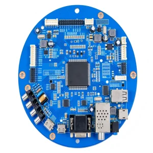


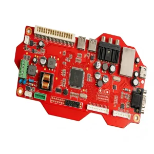

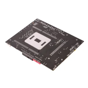

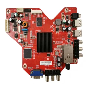
A rigorous examination of supply chain velocity, miniaturization pressures, localized sourcing ecosystems, and operational resilience across international electronics markets.
The worldwide market for Printed Circuit Board Surface Mount Device (PCB SMD) Assembly has shifted from conventional component placement to high-density, automated systems engineering. As computing architectures push deeper into peripheral edge nodes, automotive traction inverters, advanced wireless communications, and mission-critical medical robotics, the demand for precision Surface Mount Technology (SMT) has expanded exponentially. The global electronics manufacturing services (EMS) sector surpasses USD 600 billion in valuation, driven predominantly by China's comprehensive electronics supply chain in the Greater Bay Area, with Shenzhen serving as the core operational epicenter.
Modern Original Equipment Manufacturers (OEMs) and product developers no longer evaluate a China PCB SMD Assembly factory strictly on labor arbitrage. The contemporary evaluation criterion centers on Total Cost of Ownership (TCO), systemic responsiveness, technical competence across 01005 (0402 metric) and 008004 discrete geometries, and the institutional maturity of quality management systems such as IATF 16949, ISO 13485, and IPC-A-610 Class 3 compliance. In this high-throughput environment, top Chinese SMD assembly hubs maintain unmatched vertical integration, combining bare-board fabrication, automated multi-feeder pick-and-place arrays, nitrogen-purged reflow ovens, and 3D automated optical inspection (AOI) within unified production perimeters.
Shenzhen's ecosystem delivers raw laminates, microcontrollers, passive components, and specialized tooling within hours. This compressed supply loop reduces prototype iteration cycles from months to days.
Employing closed-loop solder paste printing, 3D SPI (Solder Paste Inspection), multi-angle 3D AOI, and high-resolution industrial CT X-ray inspection to eliminate solder voiding, bridging, and coplanarity issues.
Modular line architectures switch rapidly between low-volume, high-mix (LVHM) functional engineering pilot runs and multi-million-unit consumer or automotive production runs without quality deviation.
Engineering advancements in micro-pitch placement, advanced reflow thermodynamics, solder paste metallurgy, and AI-assisted defect prevention.
The electronic component footprint is experiencing radical physical compression. Passive resistors and capacitors in 0201 (metric 0603) and 01005 (metric 0402) packages are commonplace across smartphone, RF module, and hearing aid assemblies. Ultra-dense Ball Grid Arrays (BGAs) with ball pitches below 0.35 mm and Quad Flat No-Lead (QFN) packages with exposed thermal dies demand sophisticated stencil aperture engineering and tightly calibrated thermal profiles.
Over 70% of SMD solder anomalies originate during solder paste application. In-line 3D SPI systems measure paste volume, area, height, and registration in real time, automatically feeding offset adjustments back to the stencil printer.
10 to 12 heating zone convection ovens operating under an inert Nitrogen (N2) blanket hold oxygen levels under 50 ppm. This eliminates intermetallic oxidation, minimizes tombstoning, and maximizes wettability on leadless chips.
Layer counts exceeding 24 layers with laser micro-vias, via-in-pad plated over (VIPPO) structures, and fine traces down to 2.5 mil/2.5 mil line width/spacing enable direct breakout of multi-thousand-pin SoC and FPGA dies.
Automated jet dispensing of epoxy underfills protects fine-pitch BGAs from thermal-shock fatigue and mechanical shear, while selective automated conformal coating guards against atmospheric sulfur and moisture.
| SMD Assembly Technical Parameter | Standard Capability | Advanced / High-Density Capability | Quality Verification Protocol |
|---|---|---|---|
| Minimum Component Package | 0201 Imperial (0603 Metric) | 01005 & 008004 Ultra-Micro Chips | High-Magnification Optical & 3D AOI |
| Fine Pitch Placement (BGA/QFP) | 0.40 mm pitch | 0.30 mm pitch / 0.15 mm micro-bump | 3D AXI (X-Ray) Voiding Analysis (<10%) |
| PCB Dimensions Handled | 50 mm × 50 mm up to 510 mm × 460 mm | Flexible FPC up to 1200 mm long strips | Laser Warpage Sensing & Vacuum Carrier |
| Substrate Chemistries & Types | FR-4 (Tg 140°C - 170°C), CEM-3 | Rogers High-Frequency, Polyimide Flex, Metal-Core | Differential Impedance (TDR) Testing |
| Placement Accuracy (Cpk ≥ 1.33) | ±0.035 mm | ±0.015 mm with Real-Time Vision | Statistical Process Control (SPC) Monitoring |
How China SMD factories solve extreme thermal, vibrational, and electrical performance constraints across tier-one sectors.
Vehicle Control Units (VCUs), Battery Management Systems (BMS), and Motor Control Units (MCUs) undergo intense thermal cycling (-40°C to +125°C) and violent mechanical vibrations. SMT assembly requires high-lead-free liquidus solder alloys, void-free power MOSFET mounting, conformal silicone potting, and IATF 16949-audited lot traceability.
Ultrasound probes, biosensor front-ends, and portable ECG monitors demand pristine signal integrity, zero electromagnetic interference (EMI), and cleanroom SMD assembly. ISO 13485 certification governs class-clean production, strict flux residue wash limits, and automated functional parameter burn-in.
Industrial gas detection arrays, programmable logic controllers (PLCs), and environmental monitoring systems require robust transient voltage surge suppression (TVS), thick copper power distribution planes (up to 4 oz), and heavy-duty selective soldering to interface securely with high-power relay terminals.
The operational framework transforming bill-of-materials (BOM) files and Gerber datasets into market-ready finished hardware.
Before metal hits copper, our 50+ engineers execute thorough Design for Manufacturability (DFM) and Design for Assembly (DFA) audits. We verify pad clearances, stencil aperture aspect ratios, component spacing for nozzle clearance, and thermal relief geometry to optimize first-pass yields.
With direct vendor links across Arrow, Avnet, Digi-Key, Mouser, and authorized tier-1 semiconductor manufacturers, our supply chain guarantees 100% genuine components with full traceability, supported by X-ray die analysis and decapsulation verification for hard-to-source components.
Beyond SMT pick-and-place, our Bao'an facility executes firmware flashing, ICT (In-Circuit Testing), FCT (Functional Testing using custom pogo-pin test fixtures), cable assembly, mechanical housing integration, and final retail packaging under one unified MES tracking system.
Our senior engineering team reviews your Gerber archives, pick-and-place centroid data, and BOM files to deliver an actionable DFM feasibility and cost-down report within 24 hours.
Detailed technical answers addressing supply chain risks, quality control gates, intellectual property security, and manufacturing tolerances.
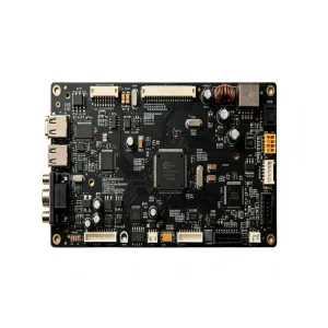
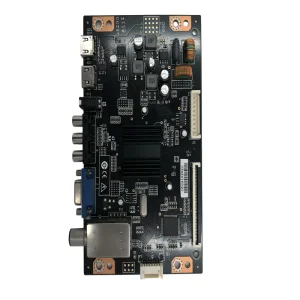
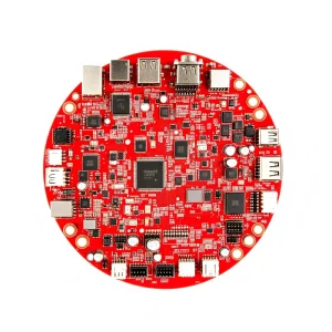
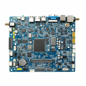
Showcasing specialized assemblies including high-efficiency switching power supplies, PoE injectors, automotive TCU units, and water safety telemetry systems.


Our operations in Bao'an District, Shenzhen run strictly under third-party validated quality management systems.
Stringent automotive defect prevention, statistical process control, and APQP/PPAP manufacturing governance.
Comprehensive medical device management ensuring strict risk analysis, cleanroom hygiene, and device history records.
Foundational quality management structure governing continuous improvement, calibration, and vendor auditing.
Environmental compliance ensuring RoHS lead-free soldering and low VOC emissions across our chemical cleaning processes.
