Explore our precision-manufactured PCBA modules fabricated using state-of-the-art laser-cut stencils and advanced solder paste deposition inspection (SPI).
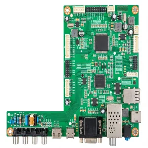
OEM LED High Bay PCB Assembly--STHL Manufacturer, Manufacturers
View PCBA Details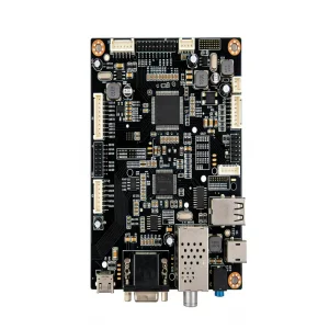
High-Quality TV LED Backlight PCB Assembly--STHL Service, Factories
View PCBA Details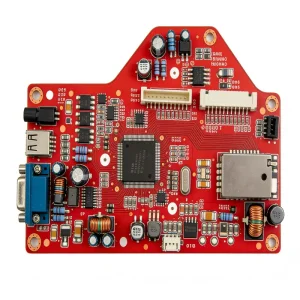
China Camera PCB Assembly PCB Assembly-1 Manufacturers, Factories
View PCBA Details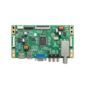
OEM LED Matrix Board PCB Assembly--STHL Manufacturer, Service
View PCBA Details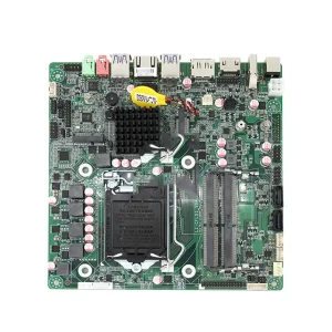
High-Quality Biological Monitoring System PCB Assembly--STHL Manufacturer, Manufacturers
View PCBA Details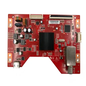
China LED Display Board PCB Assembly--STHL Manufacturers, Service
View PCBA Details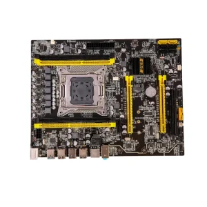
High-Quality MRI Imaging System PCB Assembly--STHL Manufacturers, Factory
View PCBA Details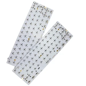
OEM LED PCB Assembly: Revolutionizing Lighting Technology with Precision and Performance Service, Factories
View PCBA DetailsOver 65% of all surface-mount assembly defects originate at the solder paste printing stage. Optimizing stencil aperture geometry, foil metallurgy, and nano-coatings directly impacts SMT line throughput and final field reliability.
In ultra-fine-pitch component assembly (down to 01005 passives and 0.3mm BGA architectures), traditional chemical etched stencils fail to provide consistent release volumes. As a specialized China PCB stencil manufacturer and EMS factory, STHL integrates fiber-laser cutting with plasma electropolishing and hydrophobic liquid-phase nanocoating to increase paste release efficiency from the standard 60-65% up to 88-95%, virtually eliminating solder bridging and insufficient solder joint defects.
Fabricated using specialized high-tensile SUS304 and SUS430 stainless steel sheets. Laser-cut stencils offer precision taper angles (typically 1 to 2 degrees) to promote instantaneous solder paste detachment during vertical separation cycles.
Created via atom-by-atom electrolytic deposition. Offers atomic-smooth aperture walls and the lowest coefficient of friction, ideal for ultra-miniature 03015/01005 passives, wafer-level chip scale packages (WLCSP), and high-frequency RF shields.
A sub-micron organosilicon or fluoropolymer barrier layer bonded chemically to the foil's bottom surface and aperture sidewalls. Repels flux resins, reduces print wipes by up to 60%, and completely halts solder ball cross-contamination.
To comply with IPC-7525B standards, precise Area Ratio (AR > 0.66) and Aspect Ratio (> 1.5) must be systematically maintained across varied component footprints on the same board layer.
| Feature Parameter | Standard Laser Cut | Laser Cut + Electropolished | Nano-Coated Laser / E-Form |
|---|---|---|---|
| Foil Thickness Options | 0.08mm - 0.30mm (3 - 12 mil) | 0.06mm - 0.25mm (2.5 - 10 mil) | 0.03mm - 0.20mm (1.2 - 8 mil) |
| Minimum Aperture Width | 0.12mm (4.7 mil) | 0.09mm (3.5 mil) | 0.05mm (2.0 mil) |
| Aperture Dimensional Tolerance | ±7 μm | ±4 μm | ±2 μm |
| Aperture Positional Accuracy | ±10 μm | ±8 μm | ±5 μm |
| Sidewall Roughness (Ra) | 1.2 - 1.8 μm | 0.5 - 0.8 μm | 0.05 - 0.2 μm (Atomic Surface) |
| Minimum Area Ratio (IPC-7525) | ≥ 0.66 | ≥ 0.60 | ≥ 0.50 (Proven Process) |
| Recommended Pitch Limit | ≥ 0.50mm BGA / QFP | ≥ 0.40mm BGA / QFN | ≤ 0.30mm Ultra-Fine BGA |
International electronics OEMs face mounting pressures: tightening margins, component lead-time anomalies, and micro-defect rates causing excessive field failures. How factory-direct stencil integration solves this dilemma.
Western and regional European EMS providers incur substantial recurring expenses on customized stencil tooling. Partnering directly with a consolidated Shenzhen manufacturer offers tooling turnaround within 12-24 hours at 40-70% lower capex.
Stand-alone stencil vendors cut files blindly as received. At STHL, our tooling engineers cross-validate the stencil aperture design directly against our internal SMT lines and 3D SPI logs, preempting bridging before copper ever meets solder.
Every laser stencil is marked with Datamatrix serialization, batch metallurgy certs, and tension maintenance records. Mesh tensions are maintained at >35 N/cm, avoiding foil sagging during prolonged continuous print runs of 50,000+ passes.
Mission-critical hardware demands uncompromising manufacturing compliance. From medical-grade ISO 13485 environments to automotive IATF 16949 production runs, our processes align with tier-1 requirements.
Comprehensive APQP, FMEA, and PPAP Level 3 documentation. Foil tension calibration logs and solder paste deposition metrics are retained for a minimum of 15 years.
Rigorous contamination controls, lead-free verification, cleanroom foil cleaning protocols, and complete audit trail capabilities for surgical and patient-monitoring electronics.
Aperture design specifically calibrated for Class 3 high-reliability applications, ensuring complete barrel fill in through-hole pin-in-paste (PIP) assembly workflows.
Full raw material declarations, heavy metal chemical safety screening, and environmental compliance certifications conforming to European and US market entry regulations.
Every electronics segment introduces distinct metallurgical and mechanical challenges. Our manufacturing facility designs stencils optimized for specific real-world production demands.
Challenge: Simultaneous placement of large D2PAK thermal pads and microscopic 0402 feedback circuits.
Solution: Multi-level stepped stencils (Step-Down 0.15mm to 0.10mm or Step-Up) manufactured via chemical milling followed by micro-laser finishing.
Challenge: Voiding under solid ground plane RF shielding cans causes severe impedance shifts.
Solution: Proprietary "window-pane" and cross-hatch aperture modifications reducing voiding under thermal pads below 10%, well above IPC minimums.
Challenge: Extreme footprint congestion on rigid-flex substrates prone to localized warpage.
Solution: Nanocoated nickel stencils combined with customized vacuum-nest fixture support plates to guarantee zero squeegee bleed-out.
As semiconductor packaging shifts toward System-in-Package (SiP), heterogeneous chiplets, and sub-0.2mm micro-BGAs, the demands on SMT tooling are undergoing a paradigm shift.
Transitioning from standard fiber lasers (pulse width in nanoseconds) to ultra-short femtosecond lasers. Eliminates the heat-affected zone (HAZ), eradicating micro-burrs and slag without the need for post-cut chemical deburring.
Deploying machine-learning CAD algorithms that evaluate Gerber geometries against historical SPI paste height inspection logs. The system automatically adjusts aperture reductions and corner radiusing based on exact solder paste alloy rheology.
Developing molecularly bonded hydrophobic and oleophobic surfaces capable of enduring over 100,000 wiper cycles without degradation, enabling virtually wash-free continuous printing in smart automated factories.
From mission-critical medical hardware to complex communication arrays, review more finished turnkey assemblies produced under our unified engineering infrastructure.
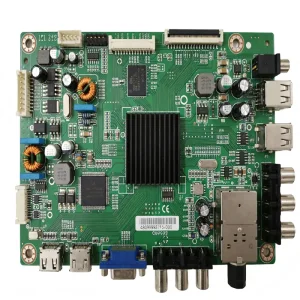
OEM Wireless Phone PCB Assembly--STHL Manufacturer, Manufacturers
View PCBA Details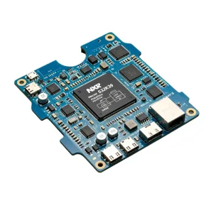
High-Quality Anesthesia Machine PCB Assembly--STHL Manufacturer, Manufacturers
View PCBA Details
High-Quality Communication PCBA Application: Connecting the World with Precision Manufacturers, Factory
View PCBA Details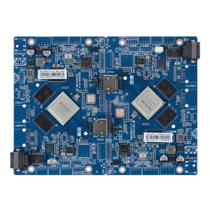
China Consumer Electronics PCBA Application: Powering the Devices of Tomorrow Manufacturer, Service
View PCBA Details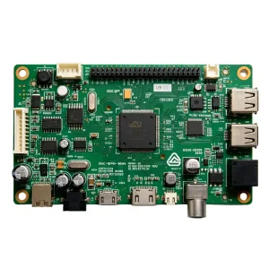
China Load Balancer PCB Assembly Service, Factory
View PCBA Details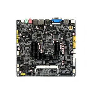
OEM AC-DC Converter PCB Assembly--STHL Manufacturer, Service
View PCBA Details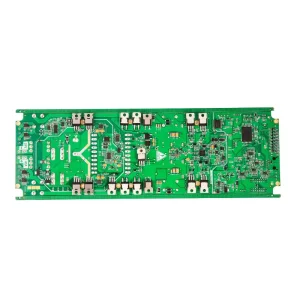
High-Quality Gas Leak Alarm PCB Assembly--STHL Service, Factories
View PCBA Details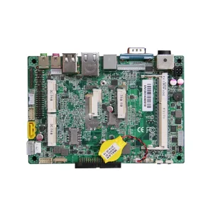
OEM Modem PCB Assembly--STHL Manufacturer, Manufacturers
View PCBA DetailsIn-depth technical answers addressing engineering tolerances, stencil frame dimensions, turnaround lead times, and global shipping protocols.
