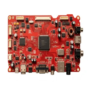
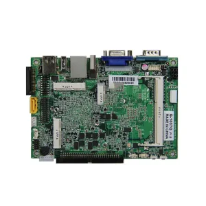
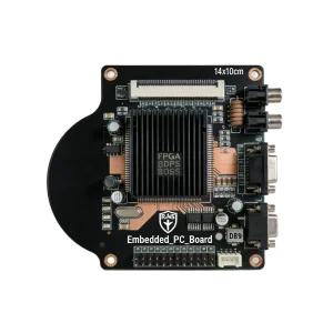
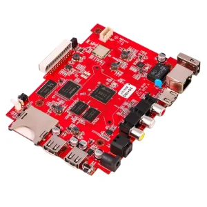
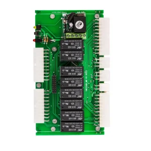
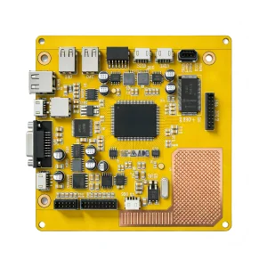
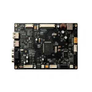
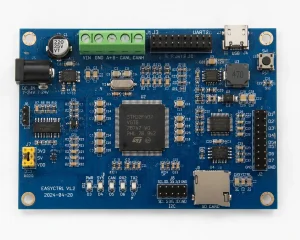
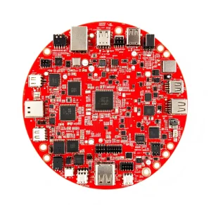
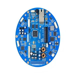
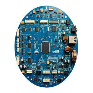
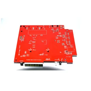
Engineered to mission-critical standards. Browse verified solutions deployed across automotive domain controllers, healthcare robotics, and distributed clean-energy grids.
Moving far beyond simple board soldering: How China's digitalized SMT infrastructure provides global brands with unprecedented structural efficiency, component engineering, and speed-to-market.
Modern Chinese electronics factories integrate component lifecycle predictive management, high-speed multi-axis pick-and-place precision (01005 chips, micro-BGAs down to 0.35mm pitch), and turnkey box-build within a single, audited Quality Management Framework.
Equipped with dual-lane automated 3D SPI (Solder Paste Inspection), online 3D AOI, inline selective soldering stations, and automated high-resolution AXI (X-Ray Inspection) validating hidden solder joints in dense multi-layer substrates.
Eliminating minimum order constraints (No MOQ policy). Startups and global enterprises can iterate complex functional prototypes seamlessly and ramp up to millions of mass-production units using identical machine programming lines.
In an unpredictable macroeconomic environment, geographic co-location and raw material proximity remain the ultimate hedges against manufacturing delays and cost inflation.
Located in Shenzhen's core industrial hub, raw substrates, high-Tg prepregs, active ICs, passive passives, precision injection molds, and metal chassis are sourceable within hours, reducing cycle latency by weeks.
Dynamic cross-referencing of 500,000+ active parts. Dedicated component engineers suggest drop-in pin-to-pin equivalent components for legacy, sole-sourced, or hard-to-find chips, protecting continuity.
Every single board moving across the assembly line carries a laser-etched 2D Data Matrix identifier linking directly to machine feeder logs, solder paste batch chemistry, reflow temperature profiles, and visual inspection data.
Daily direct dispatches via DHL, FedEx, UPS, air freight forwarding, and multimodal ocean routes ensure predictable delivery milestones across 90+ countries with custom clearing documentation and bonded warehousing support.
Granular capability metrics verified across high-volume surface mount technology lines and automated optical testing suites.
| Capability Parameter | Standard Baseline | Advanced / High-Precision Threshold |
|---|---|---|
| Layer Count (Rigid / Flex / Rigid-Flex) | 1 – 16 Layers | Up to 64 Layers (Any-Layer HDI, Micro-Vias, ELIC) |
| Smallest SMD Component Placement | 0201 (Imperial) / 0603 (Metric) | 01005 and 03015 Micro-chip Packages |
| Fine Pitch Devices (BGA / QFP / CSP) | Pitch ≥ 0.4 mm | Pitch ≥ 0.25 mm with 100% 3D X-Ray Inspection |
| PCB Board Dimensions (Max / Min) | 50 mm × 50 mm / 510 mm × 460 mm | Maximum continuous panel size up to 1200 mm (LED Arrays) |
| Substrate Chemistry Types | Standard FR-4, Lead-Free HASL, ENIG | Rogers, Polyimide (Flex), Aluminum Core, Ceramic, High-Tg, Halogen-Free |
| Testing Methodologies | Visual QA, ICT (In-Circuit), Flying Probe | Inline 3D SPI, 3D AOI, Automated 3D AXI, FCT Jigs, Burn-in Environmental Chambers |
| Soldering Technology Standards | RoHS / REACH Compliant Solder | Vacuum Reflow, Nitrogen Atmosphere (N2), Conformal Coating (Polyurethane/Silicone) |
How China-manufactured PCBA hardware conforms to international mechanical, electrical, and regulatory environments worldwide.
Rigorous conformance to IATF 16949 standards, high-vibration resilience, thermal dissipation management for battery management systems (BMS), inverter systems, and connected ADAS edge nodes.
Compliant with ISO 13485 quality protocols, cleanroom SMT environments, automated trace records for infusion pumps, telemetry units, dialysis systems, and biosensors demanding ultra-low failure rates.
Heavy-copper substrates, robust ESD protection, conformal coating against harsh moisture and sulfur compounds, driving PLCs, CNC controllers, servo drivers, and isolated power electronics.
Impedance-controlled PCB assemblies featuring dielectric core materials for multi-gigabit Ethernet switches, satellite communication terminals, 5G base units, and cellular IoT gateways.
How cutting-edge Chinese PCBA factories are preparing for AI edge computation, advanced SiP packaging, and carbon-neutral green electronics.
Transitioning from reactive defect discovery to proactive predictive correction. Machine-learning algorithms continuously monitor solder viscosity changes, thermal reflow variations, and solder joint formation in real time.
Adoption of System-in-Package (SiP), ultra-thin embedded passive components, and 2.5D substrate assembly directly within standard SMT processes to satisfy miniaturization demands for AR/VR and micro-medical implants.
Integration of low-temperature bismuth-tin solder alloys, 100% closed-loop aqueous cleaning fluid recycling, and ISO 14001 energy auditing protocols enabling Western OEMs to hit strict ESG carbon-footprint targets.
Ensuring frictionless collaboration with global corporate procurement via stringent governance models, multi-lingual engineering teams, and strict trade compliance.
Binding Non-Disclosure Agreements (NDAs) signed prior to RFQ review. Isolated server partitions guarantee complete confidentiality for your proprietary Gerber layouts, firmware code, and mechanical CAD models.
All manufacturing units maintain audited compliance with IPC-A-610 Class II and Class III standards, UL 94V-0 flammability ratings, RoHS Directive 2011/65/EU, REACH regulations, and conflict mineral tracking.
Dedicated international technical account managers ensure seamless overlap with US Eastern, Pacific, and European working hours, eliminating 24-hour turnaround lags during initial DFM feedback cycles.
Critical procurement, engineering, and manufacturing answers designed for hardware founders, supply chain managers, and sourcing engineers.
Scalable electronic assembly platforms ready for volume procurement, environmental stress testing, and turnkey enclosure integration.