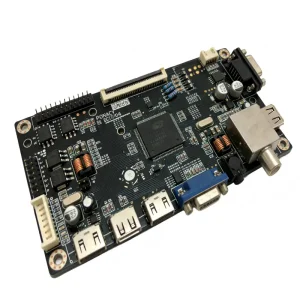
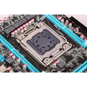
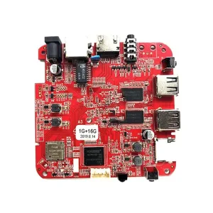
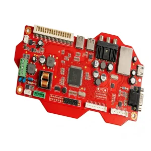
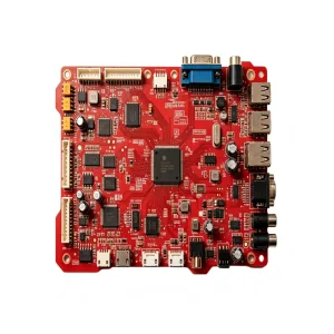
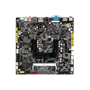
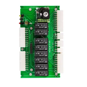
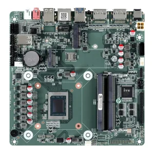
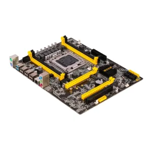
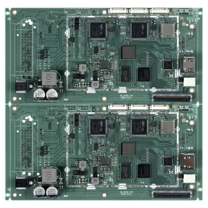
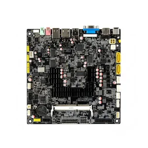
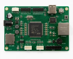
Turnkey electronic assemblies manufactured under IPC-A-610 Class 3 standards for industrial automation, renewable infrastructure, and mission-critical devices.
China remains the undisputed epicenter of global PCB and PCBA manufacturing, accounting for more than 54% of global board fabrication and electronics assembly output. Situated in Shenzhen's Bao'an high-tech corridor, Shenzhen STHL Electronics Co., Ltd. leverages this integrated industrial cluster to optimize cost structures, compress prototyping lead times, and maintain robust component pipelines.
The Greater Bay Area provides immediate physical proximity to primary copper clad laminate (CCL) producers, precision tooling shops, and world-tier component distributors. This density eliminates the international supply chain transit delays common to Western EMS facilities, cutting procurement cycles by up to 60%.
Modern Chinese electronics manufacturing has fully transitioned from labor-centric production to high-speed, automated lines. Our cleanrooms host Yamaha and Panasonic modular mounters, inline SPI, 3D AOI, and continuous nitrogen reflow ovens that ensure flawless assembly down to 01005 passives and 0.3mm BGA pitches.
Global original equipment manufacturers require strict compliance guarantees. STHL bridges international quality demands with localized production efficiency, holding accredited IATF 16949, ISO 13485, ISO 9001, and ISO 14001 certifications monitored through enterprise MES traceability systems.
Hardware procurement executives, chief supply chain officers, and engineering directors face distinct systemic challenges when sourcing electronics manufacturing services from overseas partners.
Initial quotations often obscure total landed cost due to unexpected tariff reclassifications, logistics handoffs, engineering rework fees, or batch-level scrap rates. STHL implements transparent turnkey pricing, integrating component procurement, bare board fabrication, assembly, functional testing, and customs-ready logistics under single-invoicing control to eliminate cost creep.
The integrity of embedded firmware, proprietary schematic topologies, and production Gerber design data is non-negotiable. We bind every inquiry to an enforceable Non-Disclosure Agreement (NDA) prior to receiving Gerber or BOM files. Firmware flashing runs on encrypted internal local servers with restricted, auditable engineer access logs.
Gray-market semiconductor brokerages expose assemblies to recycled, remarketed, or out-of-spec ICs. STHL maintains direct purchasing pipelines with top authorized distributors including Arrow, Avnet, Digi-Key, Mouser, and Microchip, paired with incoming X-ray, decap verification, and electrical testing to guarantee material provenance.
STHL delivers comprehensive turnkey electronic manufacturing solutions designed to streamline complex builds from initial DFM design to end-customer box-build delivery.
Before launching fabrication tooling, our 50+ engineers analyze your Gerber, centroid, and BOM data. We systematically audit solder pad geometry, trace clearance, component spacing, thermal relief, and panel arrays to prevent solder bridging, tombstoning, and copper delamination during volume runs.
Board reliability extends far beyond cosmetic solder verification. We construct customized Bed-of-Nails fixtures, in-circuit test (ICT) routines, automated optical inspection (AOI), high-voltage isolation checks, and burn-in temperature cycling programs calibrated to validate functional duty cycles before shipment.
For assemblies subjected to corrosive environments, outdoor condensation, chemical exposure, or extreme vibration, we provide robotic conformal coating (acrylic, silicone, polyurethane) with UV-curable blacklight inspection and potting containment to satisfy industrial IP67/IP68 ingress ratings.
Transition from board-level PCBA to shelf-ready finished goods without intermediate repackaging. Our 4 specialized integration lines handle precision CNC metal enclosures, injection-molded plastics, custom wire harness integration, ultrasonic welding, optical display calibration, and retail packaging.
A transparent overview of production parameters, dimensional limits, and mechanical tolerances supported at our Shenzhen electronics manufacturing facility.
| Layer Count Capability | Rigid PCB: 1–32 Layers | Flex PCB: 1–8 Layers | Rigid-Flex: 2–16 Layers | Metal Core: 1–4 Layers |
|---|---|
| Base Materials Handled | Standard FR-4, High-Tg FR-4 (Tg 170-180°C), Halogen-Free, Rogers (4350B, 4003C), Polyimide (PI), Aluminum, Copper Substrates, PTFE |
| Surface Finishes Available | HASL Lead-Free, Electroless Nickel Immersion Gold (ENIG), OSP, Immersion Silver, Immersion Tin, Hard Gold Plating (Selective Edge Connectors) |
| High-Density Interconnect (HDI) | 1+N+1, 2+N+2, 3+N+3, Any-Layer HDI via laser micro-drilling (minimum micro-via diameter 0.075mm / 3 mil) |
| Trace Width / Trace Spacing | Standard: 0.075mm / 0.075mm (3/3 mil) | Advanced/Inner: 0.05mm / 0.05mm (2/2 mil) |
| SMT Component Placement Matrix | Down to 01005 passives, 0201 chips, 0.3mm pitch ultra-fine BGA, QFN, CSP, PoP (Package-on-Package), connectors up to 150mm length |
| Soldering Technologies | Lead-Free Nitrogen (N2) Reflow, Dual-Wave Selective Soldering, DIP Through-Hole Insertion, Ultrasonic Cleaning, Hand Soldering for Sensitive Optics |
| Inspection & Verification | Inline 3D Solder Paste Inspection (SPI), Inline 3D Automated Optical Inspection (AOI), 2.5D/3D X-Ray Inspection, In-Circuit Testing (ICT), Functional Test (FCT) |
| Quality Accreditations | IATF 16949 (Automotive), ISO 13485 (Medical Devices), ISO 9001 (Quality), ISO 14001 (Environmental Management), IPC-A-610 Class 2 & Class 3 |
As electronic systems trend toward extreme miniaturization, high-frequency operation, and high-voltage power densities, STHL continuously evolves its factory floor with active capital investments.
Integration of active IC bare dies and passive resistor/capacitor components directly inside intermediate substrate inner cores, reducing loop inductance and slashing board form factors by up to 40%.
Direct Bonded Copper (DBC) and ceramic-filled prepregs designed for Silicon Carbide (SiC) and Gallium Nitride (GaN) high-efficiency switching converters in next-gen automotive inverters.
Tight impedance control (+/- 5%) up to 77GHz–110GHz frequencies for automotive radar, satellite phased-array constellations, and enterprise 6G communications infrastructure utilizing ultra-low loss hydrocarbon CCL.
Deploying computer vision neural networks at inline 3D AOI stations to perform real-time autonomous soldering parameter corrections at the paste printer and reflow ovens, targeting near-zero-defect yields.
Partnering with a Chinese manufacturer requires robust cross-border logistical predictability, customs clearance transparency, and localized communication channels.
We provide full Delivered Duty Paid (DDP), FOB Shenzhen, or EXW arrangements. Our logistics team handles Harmonized System (HS) code assignment, export licensing, import customs clearance, and local sales tax management directly to client docks in North America, the European Union, South America, and APAC.
Every raw laminate, solder alloy, flux chemistry, and passive component processed in our workshop strictly complies with EU RoHS (Restriction of Hazardous Substances) and REACH (SVHC) directives. All fabricated bare boards carry certified UL 94V-0 flammability ratings with traceable yellow cards.
Eliminate time-zone lag. STHL assigns English-fluent project managers and bilingual hardware engineers to each global account. Whether clarifying schematic ambiguities or coordinating last-minute BOM revisions, engineering responses are committed within 4 to 12 hours.
 IATF 16949 Automotive Certified
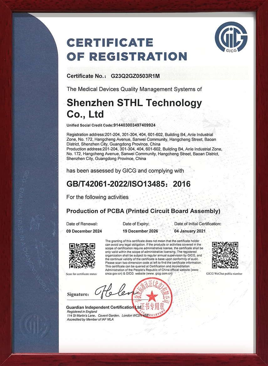 ISO 13485 Medical Devices Certified
 ISO 9001 Quality Management Certified
 ISO 14001 Environmental Certified
Direct, engineering-backed answers addressing the operational, financial, and logistical concerns of procurement directors and engineering managers.
To deliver a comprehensive turn-around proposal within 24–48 hours, our engineering desk requires: 1) Gerber RS-274X or ODB++ data containing copper, drill, soldermask, and silkscreen layers; 2) Bill of Materials (BOM) in Excel format with unique Manufacturer Part Numbers (MPN), approved second-source manufacturers, and reference designators; 3) Centroid / Pick-and-Place file (.txt, .csv); and 4) Functional Test Specifications and assembly drawings.
Counterfeit prevention is enforced at the source. We purchase 100% of semiconductors and critical passives through Tier-1 direct manufacturer lines and authorized global distributors (including Arrow, Avnet, Digi-Key, Mouser, and Future Electronics). Incoming components undergo incoming inspection protocols: packaging anti-static verification, manufacturer batch-lot code verification, X-ray leadframe inspection, and pin-level optical microscopy.
No. STHL operates a dedicated rapid-prototyping NPI (New Product Introduction) cell with zero MOQ restrictions. Clients can fabricate and assemble pilot evaluations from 1 to 5 units to confirm schematic functionality, followed by seamless transition of validated tooling, pick-and-place files, and stencil designs directly to our high-volume automated lines without requalification overhead.
Before any Gerber or schematic transmission, we execute standard Non-Disclosure Agreements (NDAs). Firmware programming occurs within an isolated factory network using pre-configured, automated production fixtures. Hex and bin files are safeguarded by cryptographic access keys; machine operators cannot extract, clone, or modify binary packages during production runs.
Every PCBA batch undergoes layered validation: 1) 3D Solder Paste Inspection (SPI) directly after stenciling; 2) Inline 3D Automated Optical Inspection (AOI) verifying polarity, alignment, solder wetting, and component values; 3) 3D X-Ray Inspection for void checks underneath BGA, QFN, and LGA pads; 4) First Article Inspection (FAI) using automated LCR systems; and 5) Tailored In-Circuit Testing (ICT) and Functional Testing (FCT) simulating working conditions.
For quick-turn prototyping, lead times can be compressed to 5 to 7 business days following material receipt and DFM clearance. Standard turnkey production runs (including 4-to-8 layer board fabrication, component sourcing, SMT/THT assembly, testing, and coating) typically complete in 2 to 3 weeks, contingent on component procurement lead times for specialized microcontrollers or FPGAs.
Comprehensive turnkey electronic assemblies for commercial networking, medical diagnostics, security monitoring, and power conversion applications.