Explore production-verified SMD board assemblies engineered across medical diagnostics, avionics, industrial edge computing, and high-frequency RF applications.
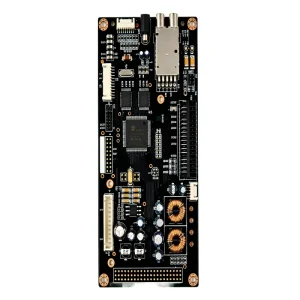
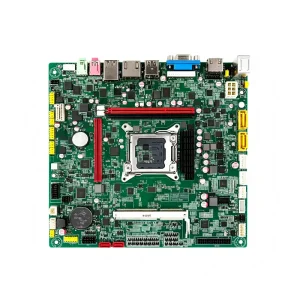

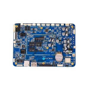
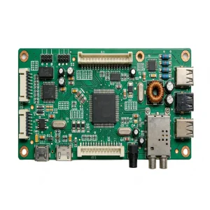
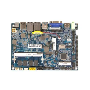
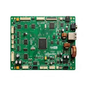
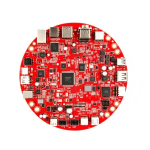
Modern Original Equipment Manufacturers (OEMs) and Tier-1 systems integrators in North America, the European Union, Japan, and Australia face acute hardware delivery hurdles: micro-component shortages, rapid lifecycle obsolescence, and hyper-dense board topologies requiring 01005 passives and ultra-fine pitch BGAs. Selecting a verified China SMD assembly manufacturer is no longer merely a low-cost sourcing decision—it is a strategic engineering partnership designed to de-risk delivery times, enforce Design for Manufacturability (DFM), and guarantee structural supply chain continuity.
Shenzhen's integrated electronics ecosystem centralizes passive discrete stockists, semiconductor agents, substrate fabs, and stencil laser cutting. This geographic density compresses NPI turns from months to days, shielding OEMs from logistical chokepoints.
Hardware enterprises demand fluid scaling: building 10 prototype iterations for pre-compliance testing followed immediately by 250,000 mass-run units. China SMD manufacturers offer agile scheduling across modular high-speed SMT lines without punitive setup fees.
Dispersing bare PCB fabrication, component sourcing, SMT placement, and functional testing creates blind spots and finger-pointing. Full turnkey EMS under a unified MES gives global hardware directors single-vendor accountability.
Process control must align strictly with application environments. Our factory lines are tuned to the precise thermomechanical and IPC classification demands of global industries.
Compliant with ISO 13485, supporting defibrillators, vital sign monitors, and infusion controllers. Automated optical inspection (3D AOI) and 100% X-ray inspection for non-destructive voiding analysis on micro-BGA packages below 15% threshold.
Certified under IATF 16949. High-reliability SMD assembly for BMS, ADAS sensing, inverter modules, and onboard telematics. Nitrogen-atmosphere reflow ovens eliminate micro-voids, and selective conformal coating shields against thermal shock and moisture.
Severe-vibration-proof SMD manufacturing for ruggedized PLCs, variable frequency drives, and edge computing gateways. Thick-copper substrates, potting, and automated conformal coating to endure chemical exposure and -40°C to +105°C thermal swings.
Controlled impedance lines, high-frequency Rogers/PTFE multi-layer stackups, and ultra-accurate component placement for 5G transceivers, Wi-Fi 7 modules, and optical transponders. Precise solder paste printing using 3D SPI prevents coplanarity bridging.
A granular look at STHL’s advanced surface-mount capabilities versus common industry norms. Engineered to satisfy stringent Tier-1 hardware specifications.
| Manufacturing Parameter | Standard Industry SMD Spec | STHL Advanced SMD Capability | Direct Buyer Benefit |
|---|---|---|---|
| Smallest Passive Component | 0402 / 0201 metric | 01005 (0402 metric) & 03015 micro | Enables ultra-compact wearable and high-density IoT footprints |
| Fine Pitch Placement (BGA/QFN) | 0.5 mm ball pitch | 0.3 mm pitch BGA, PoP (Package-on-Package) | High computational power integration in localized board regions |
| SMT Placement Accuracy | ±40 μm @ 3-sigma | ±15 μm @ 3-sigma (Fuji & Panasonic high-speed) | Eliminates component tombstoning, skewing, and bridging defects |
| Inspection Regimes | Visual / 2D AOI sampling | Inline 3D SPI + Inline 3D AOI + 3D AXI (X-Ray) | 100% defect capture prior to reflow; non-destructive hidden joint audit |
| Reflow Soldering Environment | Standard convection air | 10-Zone Reflow with Nitrogen (N2) atmosphere | Prevents metallization oxidation; minimizes micro-voids in critical BGAs |
| Bare Board Formats Handled | FR-4 standard rigid | Rigid-Flex, HDI Any-Layer, Ceramic, Metal Core (MCPCB) | Versatile thermal dissipation and flexible dynamic form factors |
| Quality Traceability | Batch / Box label tracking | MES Unit-Level 2D Barcode serialization | Complete audit trail: exact feeder, reel, operator, and reflow profile data |
How your CAD engineering data is translated into zero-defect physical hardware within our Shenzhen production facility.
Every Gerber and BOM dataset undergoes rigorous automated design rule checking. Our engineers analyze pad aspect ratios, copper balance, thermal relief geometries, and component clear-zones to catch potential assembly failures before raw materials are committed.
Using electroformed laser-cut stencils with nano-coatings, high-purity lead-free or leaded paste is applied. Inline 3D Solder Paste Inspection immediately checks height, volume, and area, halting boards with deposition anomalies before placement.
High-speed modular chip shooters place 01005 passives alongside intelligent multi-function mounters placing complex micro-BGAs, QFNs, and shielded RF enclosures. Real-time vision alignment ensures sub-20 micron placement accuracy on single and double-sided boards.
Multi-zone convection reflow with optional nitrogen gas purging ensures gradual preheating, flux activation, and controlled cooling ramps. Each board type receives a tailored reflow curve matched precisely to thermal mass and delta-T criteria across disparate component packages.
Post-reflow inspection utilizes 3D AOI for solder fillet geometry, component rotation, and coplanarity verification. High-voltage 3D X-ray systems audit BGA ball concentricity, solder ball voiding percentages, and hidden bottom-terminated component pads.
Assembled boards progress to In-Circuit Testing (ICT) via bed-of-nails or flying probe fixtures, followed by custom Functional Testing (FCT). Assemblies endure thermal cycling, burn-in stress screening, and automated conformal coating as required.
Procuring custom electronics offshore requires watertight compliance, rigorous supply chain tracing, and absolute intellectual property security.
Confidentiality agreements are signed prior to opening CAD, Gerber, or schematic data. Proprietary firmware binaries are programmed via secure, air-gapped workstations, and encrypted servers ensure your design IP stays fully protected.
Counterfeit passives and remarket ICs plague volatile markets. We source solely through direct factory franchises and authorized global distributors (Arrow, Avnet, Digi-Key, Mouser), backed by internal microscopic, decapsulation, and X-ray fluorescence audits.
Exporting to 90+ countries with full RoHS, REACH, and CE compliance documentation. Our bonded logistics teams handle DDP (Delivered Duty Paid), DAP, and multimodal priority air transit to ensure customs clearance without administrative friction.
Key technical and commercial queries resolved for procurement officers, lead hardware architects, and supply chain analysts.
We require the RS-274X or ODB++ Gerber files, an intelligent Bill of Materials (BOM) detailing manufacturer part numbers (MPNs), quantities, and package sizes, and the Pick-and-Place Centroid file (X, Y, rotation, board side). Assembly drawings and schematic PDFs are also welcomed for reference during DFM reviews.
Our dedicated procurement engineering team scans BOM lists against real-time global availability databases. When an active part encounters supply strain or End-of-Life (EOL) status, we offer drop-in pin-compatible alternatives or second-source equivalents, providing datasheets and technical change notes for engineering approval.
Yes. We operate flexible procurement models: complete full-turnkey (we source bare boards and all passives/ICs), partial turnkey (you supply proprietary programmed MCUs/ASICs while we procure passives), or full consignment (kitted components shipped directly to our Shenzhen warehouse).
Every SMD production run integrates 3D Solder Paste Inspection (SPI) to ensure consistent paste deposit volume. Post-reflow, high-density BGAs, QFNs, and LGAs undergo automated 3D X-ray inspection (AXI) to verify voiding levels remain below 15% and validate ball coplanarity in accordance with IPC-A-610 Class 3 standards.
For quick-turn prototyping with parts in stock or standard distribution, SMD assemblies can ship in as fast as 24 to 72 hours. Standard turnkey pilot builds generally require 7 to 12 working days depending on component sourcing lead times. Mass production runs are scheduled with buffer stocks and scheduled pull calls.
All finished PCBA units undergo degreasing and ultrasonic cleaning as required, followed by packaging inside static-shielding antistatic (ESD) moisture-barrier bags with desiccant packs and humidity indicator cards. Outer packaging utilizes custom-slotted antistatic foam within robust, moisture-resistant master cartons.
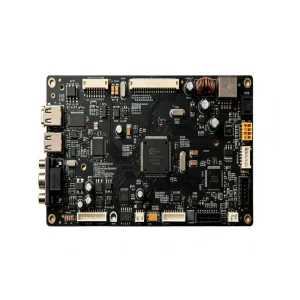
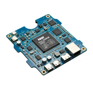
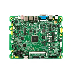
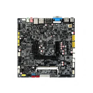
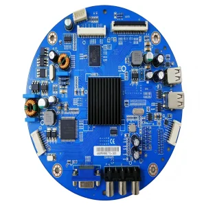
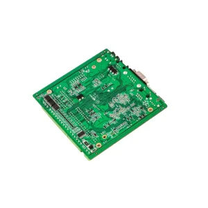
Explore additional turnkey SMD assemblies manufactured across our certified Shenzhen production lines.
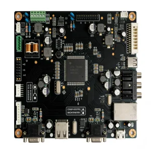
Zero counterfeit compromises. Full lot-traceability integrated directly with world-class authorized component distributors.
