Explore validated hardware manufactured with zero-defect SMT workflows, micro-BGA placement, and closed-loop automated optical and X-ray inspection.
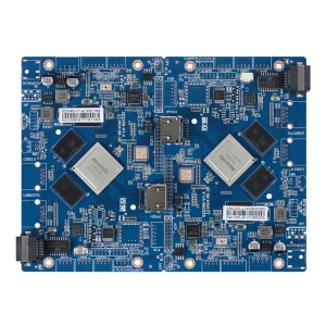
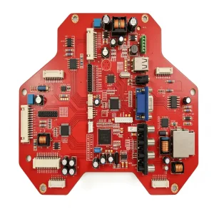
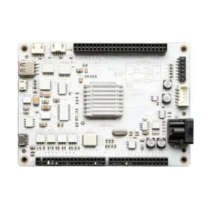
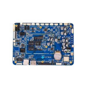
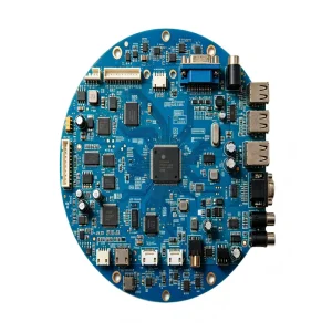


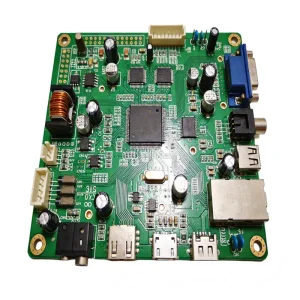
The global contract electronics manufacturing landscape has transitioned from transactional, labor-intensive placement services into sophisticated, automated, and vertically unified microelectronics hubs. Operating from Shenzhen’s core industrial clusters, a certified China Smt Board Assembly Manufacturer acts not merely as a production vendor, but as a strategic co-engineering partner navigating complex multi-layer topologies, sub-0.3mm fine pitch arrays, and mission-critical component provenance.
Shenzhen maintains unmatched geographical density across the tier-1 electronics value chain. Bare board copper clad laminates, precision laser-cut electro-polished stencils, active wafer dies, passive reel packaging, and specialty potting compounds exist within a two-hour logistics perimeter. This compression eliminates weeks of transatlantic lead time during iterative engineering pilot runs and critical NPI (New Product Introduction) cycles.
Global Original Equipment Manufacturers (OEMs) benefit from structural cost advantages without sacrificing quality integrity. Through direct authorized factory relationships with global component distributors (Arrow, Avnet, DigiKey, Mouser) and domestic direct franchised lines, material bills are audited down via systematic value engineering, alternate footprint second-sourcing, and high-speed automated placement economies of scale.
Modern China SMT assembly operates far beyond standard commercial thresholds. Advanced manufacturers maintain automated manufacturing environments compliant with IPC-A-610 Class 3 for mission-critical hardware, supported by IATF 16949 automotive zero-defect quality systems, ISO 13485 medical device life-support traceability, and ESD-controlled Class 100,000 cleanroom operational floors.
Achieving high first-pass yields across dense substrates demands micro-mechanical precision, accurate solder paste rheology, and tightly controlled thermal reflow profiling.
| Process Stage | Technical Capability Parameter | Quality Threshold / Standard | Engineering Impact |
|---|---|---|---|
| Solder Stencil Printing | Fully automatic optical alignment; 0.08mm - 0.15mm laser electro-polished foils | Cpk ≥ 1.66 @ ±12.5μm | Prevents bridging on fine-pitch 0.3mm BGA and insufficient solder on 0201/01005 passives. |
| 3D SPI Verification | 100% volumetric inline 3D solder paste height, area, and volume inspection | 100% IPC-7527 Compliance | Intercepts 70% of potential assembly anomalies prior to component mounting and reflow. |
| High-Speed Placement | Modular multi-gantry mounters; components down to 01005 (0402 metric) & PoP | ±0.025mm accuracy @ 3σ | Enables ultra-compact board architectures for IoT, wearables, and edge AI compute engines. |
| Nitrogen Reflow Soldering | 10 to 12 heating zones; lead-free SAC305 profile; <50ppm O2 closed loop | ΔT ≤ 2.5°C across board | Eliminates component warpage, head-in-pillow (HiP) defects, and guarantees intermetallic bonding. |
| Inline 3D AOI & AXI | Dual-sided multi-angle optical + transmission X-ray laminography | BGA Voiding < 15% (IPC < 25%) | Guarantees 100% hidden solder joint integrity on QFN, LGA, micro-BGA, and under-package ground pads. |
| Final In-Circuit / FCT | Custom pneumatic bed-of-nails fixtures, boundary scan (JTAG), RF spectrum validation | 99.8% Test Coverage | Validates dynamic circuit function, voltage regulators, firmware bootloader, and sensor telemetry. |
A defect discovered during prototype reflow costs ten times more than one caught in CAM engineering; a defect discovered in the field costs ten thousand times more. Our engineering team conducts comprehensive pre-production design audits before releasing panels to production.
We evaluate pad-to-trace ratios, solder mask defined (SMD) vs non-solder mask defined (NSMD) pads for BGAs, and ensure thermal relief geometry prevents passive component tombstoning during thermal equilibrium transitions.
Differential copper distribution triggers severe thermal warpage on high-layer HDI substrates. We optimize copper balance, verify stack-up symmetry, and configure break-away panel tabs to ensure planarity throughout lead-free 260°C peak temperatures.
Every Bill of Materials is cross-referenced through real-time lifecycle databases to flag End-of-Life (EOL), Not Recommended for New Designs (NRND), and excessive lead-time vulnerabilities, suggesting footprint-compatible drop-in alternatives.
Test point clearance, spacing, and distribution are vetted across power planes, critical differential signaling pairs, and digital buses to enable complete bed-of-nails in-circuit testing (ICT) and boundary scan verification without mechanical interference.
Different operational environments dictate unique substrate chemistries, assembly tolerances, conformal protection, and quality tracking protocols.
Engine management, ADAS vision processors, battery management systems (BMS), and telematics demand zero-defect durability. We implement strict PPAP documentation, thermal shock cycling (-40°C to +125°C), selective underfill, automated robotic silicone potting, and complete lot-level MES component traceability down to individual wafer batches.
Diagnostic imaging terminals, surgical camera processing units, and patient vital sign telemetry require rigorous environmental cleanliness and electrical isolation. Our manufacturing lines apply IPC Class 3 solder joint fillets, ionic cleanliness contamination checks, biocompatible conformal coating, and full DHR (Device History Record) validation.
Harsh factory automation, motor drives, environmental particle monitors, and gigabit microwave communication hardware require impedance-controlled multi-layer boards on Rogers, Taconic, or high-Tg FR-4 laminates, featuring cavity shields, micro-vias, and automated selective conformal spray against moisture and caustic chemical ingress.
As silicon architectures push thermal and spatial physical limits, SMT manufacturing converges with advanced microelectronics substrate packaging.
Universal deployment of nano-coated laser stencils, sub-micron closed-loop optics, and specialized vacuum pickup nozzles for 01005 passive arrays and wafer-level chip scale packages (WLCSP).
High-temperature, high-thermal-conductivity assembly utilizing specialized sintered silver pastes, direct bonded copper (DBC) substrates, and high-frequency planar magnetic integration for automotive power electronics.
Transition toward embedding active semiconductor dies directly within inner PCB core layers, paired with surface SMT mounting, drastically minimizing parasitic inductance and maximizing spatial volumetric efficiency.
Full Industry 4.0 dark-factory SMT automation with real-time neural network feedback connecting 3D AOI/AXI directly to solder paste printers and placement heads to self-correct solder volumes and offsets instantly.
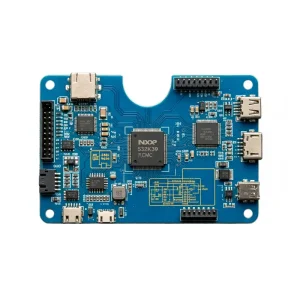
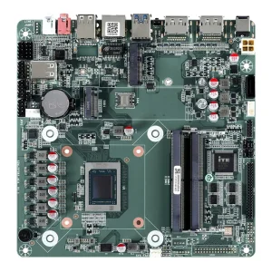
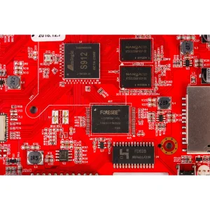
Review our specialized product realizations spaning medical ultrasound imaging, avionics reference units, industrial sensors, and ultra-high-definition video servers.


Detailed technical answers addressing core qualification parameters, equipment tolerances, DFM reviews, and supply-chain risk mitigation for global hardware engineers and sourcing directors.
To perform an exhaustive DFM analysis and generate a reliable quote, our engineering team requires: (1) ODB++ or standard Gerber RS-274X files including copper layers, solder mask, silkscreen, drill files, and board outline; (2) Detailed Bill of Materials (BOM) in Excel with manufacturer part numbers (MPN), approved alternate parts, reference designators, and package footprints; (3) Pick-and-Place (Centroid / XY coordinates) file indicating rotation angles and board origin; and (4) Assembly / Fabrication drawings documenting special requirements such as impedance control, IPC Class classification, selective conformal coating zones, and custom test instructions.
Voiding is controlled through three primary vectors: (1) Stencil Design: Implementing window-pane / segmented apertures on large central thermal ground pads to provide volatile gas egress channels during flux activation; (2) Solder Chemistry: Formulating Type 4 or Type 5 lead-free SAC305 solder pastes with optimized activator kinetics; and (3) Controlled Reflow Atmospheres: Utilizing multi-zone forced convection ovens equipped with Nitrogen inerting (<50ppm O2) and vacuum-assisted reflow (Vapor Phase / Vacuum Reflow chambers) when BGA voiding requirements demand levels below 10%, well beyond the standard 25% IPC-A-610 Class 3 baseline.
We operate a certified zero-tolerance procurement framework: Components are sourced exclusively via original component manufacturers (OCMs) or franchised Tier-1 global distributors (Arrow, Avnet, DigiKey, Mouser, Future). For hard-to-find or legacy parts requiring open-market acquisition, our internal incoming quality control (IQC) laboratory performs: (1) Decapsulation and die verification under high-magnification microscopy; (2) X-ray inspection of internal bond wires and leadframe integrity; (3) XRF elemental spectrometry testing for RoHS / lead content compliance; and (4) Solderability testing in accordance with IPC/JEDEC J-STD-002.
Yes. We enforce identical process chemistry and feeder equipment across both pilot NPI cells and high-speed multi-gantry mass production lines. Feeder calibrations, thermal profiles, stencil laser cutting tolerances, and 3D AOI inspection algorithms developed during the First Article Inspection (FAI) pilot phase are digitally captured in our Manufacturing Execution System (MES) and propagated directly into volume assembly, eliminating scale-up yield drop-offs.
We provide fully automated selective film-coating and spray dispensing systems utilizing robotic multi-axis applicators. Available chemistries include acrylics (HumiSeal 1B31 / 1B73), polyurethanes, silicones, and ultra-thin solvent-free UV-curable polymers. Automated black-light UV optical inspection verifies edge definition, ensures non-keep-out zone isolation (connectors, test points, gold fingers), and guarantees uniform dry film thickness (typically 25μm - 75μm) according to IPC-CC-830 standards.
Before examining any CAD, Gerber, or proprietary BOM documentation, we execute a legally enforceable bilingual Non-Disclosure Agreement (NDA). Customer engineering files are segmented within air-gapped on-premise servers accessible strictly by assigned project engineers via multi-factor authentication (MFA). Firmware binary flashing on the production floor is performed through encrypted automated programmers preventing firmware extraction, and all physical scrap or un-programmed ICs are quarantined and shredded under strict supervisory protocols.
