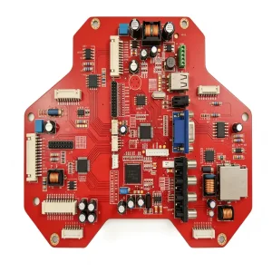
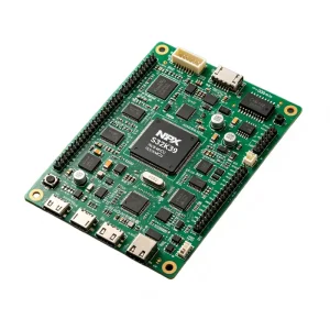
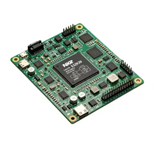
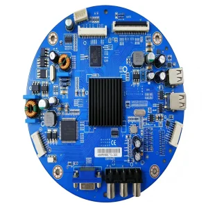
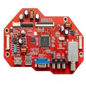
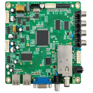
Explore real-world industrial, medical, and power management assemblies delivered with sub-millimeter precision and multi-layer traceability.
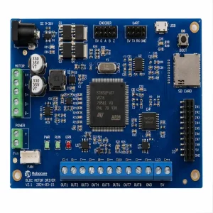
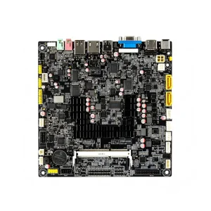
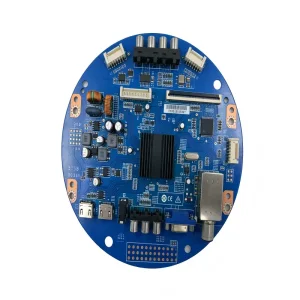

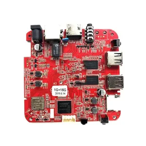
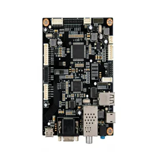
A macroeconomic and technical assessment of surface-mount electronic assembly, technological evolution, and China's strategic manufacturing role in resilient global electronics supply chains.
The global Surface Mount Technology (SMT) market continues its compound annual growth, driven by unprecedented electrification across automotive architectures, AI computing nodes, smart IoT endpoints, and renewable power converters. The proliferation of high-density interconnect (HDI) substrates and fine-pitch array packaging necessitates specialized manufacturing infrastructure capable of sub-mil mounting tolerances.
Micro-miniaturization from 0402 and 0201 passives down to 01005 and 008004 components demands closed-loop solder paste printing, automatic optical verification, and dynamic thermal compensation in multi-zone reflow furnaces. SMT factories must adopt sub-micron optical placement heads to prevent defects such as tombstoning, skewing, and solder voids.
Global OEMs no longer evaluate SMT providers strictly on pick-and-place speed (CPH). Rigorous compliance demands board-level unit tracing from bare-substrate laser serialization, raw solder lot numbers, component reel reel-ID verification, reflow temperature logs, to SPI and 3D AOI inspection records managed under intelligent Manufacturing Execution Systems (MES).
Why Tier-1 hardware developers and high-reliability OEMs consolidate their PCBA turnkey manufacturing operations in Shenzhen's hyper-dense industrial cluster.
Within a 30-kilometer radius across Shenzhen and Dongguan, STHL accesses world-class raw PCB fabricators, active silicon distributors, passives warehouses, custom heatsink CNC toolmakers, and packaging manufacturers. This geographical density cuts component procurement cycles by up to 65% compared to Western counterparts.
Our dedicated procurement engineering team reviews Bills of Materials for obsolescence, extended lead times, and single-source choke points. Through direct franchise agent partnerships and secondary component tier qualification, we routinely uncover 15% to 35% cost reductions without degrading MTBF or electrical performance.
Transitioning from Gerber sign-off and BOM validation to loaded, X-rayed, and functionally verified PCBAs in as fast as 24 to 48 hours. Our dedicated NPI (New Product Introduction) engineering cells operate independent of mass-production lines, ensuring agile design verification without bottlenecking volume schedules.
Over 50 full-time hardware, DFM, process, and test fixture engineers back your build. Every work order undergoes exhaustive Design for Manufacturing (DFM) and Design for Testing (DFT) reviews, catching aperture mismatches, thermal shadows, and solder bridge risks before stencils are cut.
A transparent breakdown of how high-reliability electronic assemblies flow through our dust-free automated production lines in Bao'an, Shenzhen.
Every raw panel receives an indelible 2D DataMatrix code linked to our MES. Anti-static vacuum brush cleaners remove micro-debris and dust prior to solder application, preventing surface tension anomalies.
Fully automatic solder paste printers utilize electroformed nickel stencils with fiducial camera alignment. Squeegee speed, angle, and paste replenishment are digitally regulated to ensure uniform deposition across pads.
In-line 3D laser profilers calculate solder paste volume, height, area coverage, and offset on 100% of pads. Solder bridging, insufficiency, and dog-ears trigger automated line halts before component placement.
Dual-lane, high-speed mounters place ultra-small 0201/01005 passives at up to 80,000 CPH, followed by multi-function heads mounting fine-pitch BGAs, QFNs, micro-connectors, and odd-form components with optical verification.
10-zone reflow ovens running under controlled nitrogen (N₂) atmospheric blankets protect against intermetallic oxidation. Distinct thermal profiles are calibrated for SAC305 lead-free pastes, preventing tombstoning and delamination.
Dual-angle 3D AOI flags dry joints, polarity inversions, missing parts, and lifted leads. High-density BGA, LGA, and QFN footprints undergo high-resolution 3D X-ray inspection to guarantee solder void ratios remain strictly under 15%.
For through-hole power components, electrolytic capacitors, and heavy industrial terminals, precision selective wave soldering fixtures protect pre-assembled SMT passives while yielding flawless barrel-fill wetting.
Every PCBA undergoes In-Circuit Testing (ICT) via bed-of-nails or flying probe, followed by functional programming (FCT) and environmental stress testing. Robotic selective spray coating applies UV-curable silicon or acrylic protection.
Comprehensive tolerance thresholds, machinery specifications, and process parameters configured for mission-critical hardware builds.
| Process Parameter | Production Capability & Equipment Standards | Quality Verification Baseline |
|---|---|---|
| Placement Capability & Sizes | Passives down to 01005 (0402 metric), active silicon down to 0.3mm BGA ball pitch, ultra-fine pitch QFP down to 0.3mm | Multi-camera optical centering, closed-loop fiducial mark tracking |
| Placement Accuracy | Chips: ±0.035mm (3 sigma); QFP/BGA: ±0.025mm (3 sigma) | In-line post-placement 3D AOI verification |
| PCB Dimensions & Thickness | Min: 50mm × 50mm; Max: 510mm × 460mm; Board Thickness: 0.2mm to 4.5mm | Automated conveyor width adjustment, anti-warpage clamping |
| Substrate Compatibility | FR-4 (Standard & High-Tg), Aluminum IMS, Flexible FPC, Rigid-Flex, Rogers High Frequency, Ceramic Substrates | Pre-baking moisture degassing ovens (IPC/JEDEC J-STD-033) |
| Reflow Thermal Profile | 10 heating zones + 2 cooling zones, Nitrogen (N2) atmosphere capable, residual O2 < 500 ppm | KIC thermal profiling dataloggers calibrated per project BOM |
| Solder Void Inspection (BGA/QFN) | Off-line / In-line high-penetration 3D X-Ray Inspection (AXI) | IPC-A-610 Class 3 compliant: Void area ratio < 15% (Custom < 10%) |
| Testing Methodologies | Flying probe test, In-Circuit Test (ICT), Flash / MCU programming, Functional Test (FCT), Burn-in room testing | Custom pneumatic test fixtures, LabVIEW automated test software |
| Quality Certifications | IATF 16949 (Automotive), ISO 13485 (Medical), ISO 9001 (Quality), ISO 14001 (Environmental) | Annual independent external audits, 100% full MES traceability |
Engineered to conquer harsh operational environments, stringent regulatory frameworks, and extended operational lifecycles.
Demanding absolute zero-defect manufacturing for Telematics Boxes (T-Boxes), Battery Management Systems (BMS), inverter controllers, and LiDAR sensor processing boards. Assemblies withstand high vibration, wide thermal ranges (-40°C to +125°C), and thermal cycling under automotive validation protocols.
From portable ultrasound scanners and medical barcode scanners to multi-parameter ward monitoring devices. Built with medical-grade clean room SMT lines, zero-flux contamination washing, anti-static handling, and lot-level medical component traceability.
Robust PLC controllers, motor drive boards, environmental restoration telemetry loggers, and boost converters designed for 24/7 continuous operation. Engineered with thick copper boards, precision potting, conformal coating, and strict creepage/clearance electrical compliance.
How international hardware enterprises de-risk offshore manufacturing contracts and achieve stable, multi-year production yields.
Global procurement teams prioritize vendors that perform proactive design reviews before PO generation. Validating solder mask clearances, pin-to-hole aspect ratios, and test pad accessibility eliminates expensive prototype respins.
Modern enterprises increasingly adopt hybrid procurement: consigning proprietary programmed ASICs or specialized FPGAs while delegating standard passive resistors, capacitors, connectors, and power ICs to the China factory's high-volume supply chain.
Securing IP begins before quotation via bilateral NDAs. At STHL, customer firmware is downloaded directly via encrypted offline programming stations, isolated from factory network access, and test logs are backed up with cryptographic hashes.
Hardware startups and enterprise R&D teams avoid capital lockup through zero minimum order quantity (No MOQ) policies. Validating an initial 5-piece prototype batch on the exact automated SMT line utilized for 100k-unit production guarantees seamless transition.
Comprehensive engineering, quality, and commercial answers to frequent questions asked by overseas hardware directors and sourcing specialists.
Advanced SMT, cable harnessing, box build, and specialized telemetry PCBA manufactured for global enterprises.