Explore production-proven turnkey surface mount PCB assembly units across power conversion, vision telemetry, medical electronics, and sensory networks.

Analyzing how world-class component ecosystems, sub-micron automated SMT equipment, and engineering agility converge to deliver unrivaled Total Cost of Ownership (TCO).
Shenzhen and the broader Pearl River Delta provide an unmatched radius of passive suppliers, semiconductor franchised distributors, bare-board laminators, and tooling specialists. Sourcing components within a 2-hour logistics perimeter minimizes replenishment friction and prevents lead-time spikes.
Modern Chinese SMT factories invest heavily in industry-leading Fuji, Yamaha, and ASM pick-and-place lines capable of ultra-high-speed chip shooting (up to 100,000 cph) with optical laser correction, dual-lane conveyor systems, and 10-zone nitrogen reflow ovens ensuring zero thermal warpage.
Adherence to global engineering standards separates tier-one Chinese factories from low-end workshops. Certified management ecosystems guarantee reproducible process yields for mission-critical sectors without compromise.
A rigorous overview of inspection gates, soldering physics, substrate metallurgy, and precision placement capabilities deployed across our Chinese manufacturing floor.
Over 70% of SMT soldering defects originate during the stencil printing phase. Our factory enforces inline 3D SPI to evaluate solder paste volume, height, area, and bridging risks prior to component placement.
Utilizing multi-zone reflow profiles purged with high-purity Nitrogen (N2) lowers oxygen levels below 500 ppm, drastically cutting solder surface oxidation, curbing micro-voiding in leadless QFNs, and enhancing intermetallic bonding.
Post-reflow inspection combines high-speed multi-angle 3D Automated Optical Inspection with deep 2D/3D X-Ray transmission to detect hidden BGA solder balls, micro-bridging, head-in-pillow (HiP) defects, and solder voids below 10% threshold.
For high-vibration automotive control units and extreme humid environments, automated selective robotic dispensing lines apply silicone, acrylic, or polyurethane conformal coatings with UV blacklight fluorescent validation.
| SMT Technical Parameter | Standard Capability | Advanced / High-Precision Range | Quality Verification Standards |
|---|---|---|---|
| Min Component Pitch / Size | 0201 passives, 0.4mm pitch ICs | 01005 chips, 0.3mm ultra-fine pitch BGA/WLCSP | Laser positioning & Telecentric Optical Sensing |
| PCB Layer Count & Form Factor | 2 to 16 Layers FR-4 Rigid | Up to 48 Layers, Rigid-Flex, HDI Any-Layer, Metal Core | IPC-6012 Class 3, Impedance verification ±5% |
| Max / Min PCB Dimensions | 50mm x 50mm to 450mm x 500mm | Sub-miniature (8mm x 8mm) to Large Backplanes (650mm x 600mm) | Edge-rail clamping, dual-side de-paneling routed |
| BGA Voiding Ratio Control | < 15% Area Voiding | < 8% Medical & Automotive Class 3 Standard | 3D Computed Tomography / Real-time AXI |
| Solder Alloys Applied | SAC305 (Sn96.5Ag3.0Cu0.5) Lead-Free | High-reliability alloys (Sn/Pb, Indium, Low-temp Bi alloys) | RoHS 3 (2015/863/EU), REACH (EC 1907/2006) |
Tailored Surface Mount Technology deployments engineered to withstand severe thermal swings, vibration profiles, and rigorous functional lifecycles.
Modern electric vehicles rely on fault-tolerant Vehicle Control Units (VCU) and Battery Management Systems (BMS). Our IATF 16949 lines implement PPAP Level 3 documentation, automated optical pin inspection, and 100% burn-in thermal cycling to eliminate latent road failures.
With life-critical reliability at stake, our ISO 13485 certified cleanroom assembly lines support surgical instruments, patient anesthesia monitors, and sub-miniature digital hearing aids requiring clean ionic contamination metrics (<0.75 µg/cm² NaCl equivalent).
Field controllers operating in power utilities, robotic workcells, and oil/gas pipelines demand extreme robustness against surges, electromagnetic interference, and wide operating thermal envelopes (-40°C to +105°C).
How our Shenzhen manufacturing headquarters shields North American, European, and Asia-Pacific OEM partners from silicon shortages, obsolescence, and intellectual property leaks.
We source exclusively through authorized franchised channel partners and original component manufacturers (OCM). When obsolete components must be acquired on the open spot market, our internal quality lab conducts rigorous incoming inspections.
Design teams frequently face unexpected End-of-Life (EOL) or Last-Time-Buy (LTB) notifications during active production. Our procurement engineers constantly screen Bills of Materials (BOM) against global market availability database engines.
Protecting intellectual property is non-negotiable. We implement strict digital air-gapping, customized Non-Disclosure Agreements (NDA) under enforceable commercial frameworks, and encrypted on-chip flashing stations.
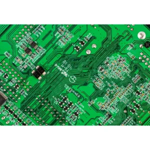
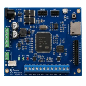
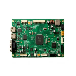
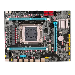
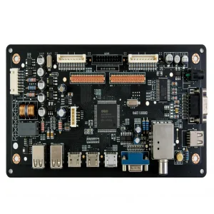
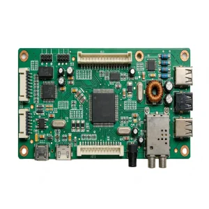
Review our specialized assemblies engineered for mission-critical aerospace indicators, high-speed computing modules, automotive ECUs, and consumer wireless nodes.

In-depth responses covering thermal profiling, moisture control, stencil engineering, testing fixtures, and production logistics.
All sensitive active components (IC, BGA, QFN) are controlled strictly according to IPC/JEDEC J-STD-033 standards. Components are vacuum-sealed with desiccant and humidity indicator cards. Any parts exposed beyond their floor life rating (e.g., MSL 3 exceeding 168 hours) undergo computer-controlled baking ovens at 125°C before feeder loading to prevent popcorn cracking during reflow.
For chips down to 0201 or BGAs with pitch <0.4mm, standard chemical etched stencils fail to provide clean solder release. We utilize high-precision electro-polished laser cut stainless steel stencils or nickel-plated FG (fine-grain) stencils with specialized nano-coatings. This decreases surface tension, ensuring a consistent aperture transfer efficiency >90%.
Yes. Our Shenzhen facility operates 7 modern high-speed SMT lines alongside 2 dedicated selective wave soldering and dual-wave soldering lines. Heavy connectors, transformer blocks, and electrolytic capacitors with through-hole leads are soldered using precision CNC titanium pallets to prevent thermal shock to nearby surface-mount parts on the bottom side.
Tombstoning on 0201/01005 passives is prevented by balancing pad thermal relief traces and profiling reflow soak phases precisely to minimize surface tension differentials. For BGA packages, we fine-tune our 10-zone reflow temperature ramp rates and deploy vacuum-assisted reflow soldering or nitrogen environments, guaranteeing BGA ball voiding remains well beneath the 10% IPC Class 3 threshold.
Beyond standard 3D SPI, 3D AOI, and X-ray, we engineer project-specific test jigs: In-Circuit Testing (ICT), Flying Probe tests for unpopulated prototypes, boundary scan (JTAG), and custom Functional Circuit Testing (FCT) simulating actual operating voltages, clock frequencies, communication handshakes, and peripheral loads.
To deliver an audit-ready DFM and comprehensive turnkey quotation, we need: 1) Gerber files (RS-274X or ODB++ format), 2) Structured BOM indicating manufacturer part numbers (MPN), reference designators, and package descriptions, 3) Centroid (Pick-and-Place / XY Coordinates) file, and 4) Assembly drawing or testing requirements specification.
