Pioneering Zero-Defect Electronic Manufacturing Services (EMS): Integrating Multi-Angle 3D AOI, Telecentric Optics, AI Deep-Learning Defect Classification, and Full IPC-A-610 Class 3 Industrial Rigor.
Engineered and audited through continuous Automated Optical Inspection, 3D SPI, and automated functional diagnostics across specialized automotive, medical, and industrial sectors.

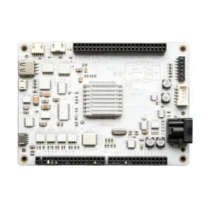
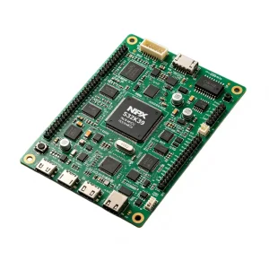
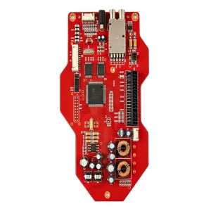
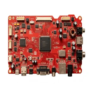
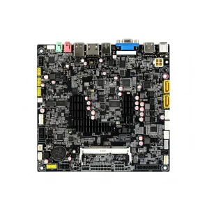
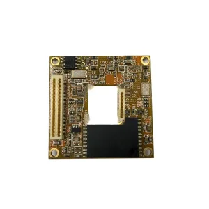
As electronic packages shrink toward ultra-miniaturized 01005 passives and 0.3mm-pitch Ball Grid Arrays (BGAs), traditional manual inspection is rendered obsolete. Modern Automated Optical Inspection (AOI) within world-class PCBA facilities has shifted from a post-reflow sorting filter to a closed-loop cyber-physical process control engine.
Traditional 2D AOI relies solely on grayscale contrast and top-down RGB illumination, leaving it vulnerable to false calls caused by PCB board flex, silkscreen reflections, and varied component markings. Modern Tier-1 manufacturers deploy 3D Multi-Frequency Moiré Fringe Interferometry, taking true height profile maps (Z-axis volumetric topology) of solder fillets down to 1 micrometer resolution to identify bridging, lifted leads, dry joints, and insufficient solder volume before boards proceed down the line.
World-class EMS lines do not relegate AOI to a single terminal checkpoint. STHL embeds high-speed AOI systems both pre-reflow (post-placement) and post-reflow. Pre-reflow AOI catches placement skew, tombstoning precursors, reversed polarities, and missing parts when components are easily repositioned without thermal stress. Post-reflow AOI then measures wetting angles, solder meniscus integrity, solder bead ejection, and intermetallic stability.
Over 65% of SMT soldering defects trace back directly to solder paste printing imperfections. By synchronizing 3D Solder Paste Inspection (SPI) data with downstream Pre/Post-Reflow AOI and pick-and-place positioning systems via unified IPC-CFX / IPC-HERMES protocols, the production line automatically offsets stencil squeegee pressure, print alignment, and placement coordinates in real time.
In Mission-Critical Systems, the Cost of SMT Defect Escapes Escalates by an Order of Magnitude (10x Rule) at Each Progressive Integration Tier.
Defect detection costs expand exponentially throughout product assembly lifecycles: catching a misaligned passive at Solder Paste Printing costs approximately $0.10; at Post-Reflow AOI inspection it costs $1.00; after through-hole hand insertion and selective soldering, $10.00; during final box-build functional testing, $100.00; and in the field following consumer or automotive delivery, the cost often exceeds $1,000 to $10,000+ due to safety recalls, warranty claims, and brand erosion. Rigorous high-throughput AOI implementation eliminates anomalies at the earliest stage.
With silicon nodes transitioning to heterogeneous chiplets and 0.4mm pitch Quad Flat No-Lead (QFN), Micro-BGA, and Wafer-Level Chip Scale Packaging (WLCSP), optical shadowing around package edges has made conventional single-camera top-down AOI inadequate. High-grade contract manufacturers have integrated multi-directional multi-color structured illumination cameras that scan simultaneously across 4 to 8 side-angle optical sensors, neutralizing line-of-sight occlusion.
Global semiconductor supply chains present severe volatility in component procurement. Integrated Optical Character Verification (OCV) and Optical Character Recognition (OCR) systems check manufacturer laser markings, lot codes, capacitor color gradations, and IC pin orientations against engineering CAD centroids. This prevents counterfeit part introduction, incorrect reel staging, and polarity inversions prior to irreversible reflow soldering.
Quantitative operational metrics comparing legacy manual optical inspection, planar 2D AOI, multi-projection 3D AOI, and Automated X-Ray Inspection (AXI) within high-yield SMT factories.
| Inspection Methodology | Core Measurement Principle | Detectable SMT Defects | False Alarm (Call) Rate | Throughput Speed | IPC-A-610 Compliance Rating |
|---|---|---|---|---|---|
| Manual Visual Inspection (MVI) | Human operator visual check via stereo microscope or magnifying ring light. | Gross component bridging, completely missing parts, heavy misalignment. | > 15.0% - 25.0% Escape | Low (< 2 cm²/sec) | Class 1 Only; Unsuitable for fine-pitch SMT |
| Planar 2D AOI | Single/multi-color RGB LED ring lights; top-down CCD/CMOS optical grayscale thresholding. | Missing parts, lateral offset, billboarding, polarity errors, basic bridging. | 1.5% - 4.5% False Call | Moderate (30 - 45 cm²/sec) | Class 2 Standard Consumer Assemblies |
| Advanced 3D AOI (Digital Fringe) | 4 or 8-way digital Moire fringe pattern projection + 12-25MP telecentric optical cameras. | True coplanarity, lifted leads (≥ 5μm), solder joint volume, dry joints, tombstoning. | < 0.15% Optimized | Ultra-High (50 - 75 cm²/sec) | IPC Class 3, Medical (ISO 13485), Automotive (IATF 16949) |
| Automated X-Ray Inspection (AXI) | Transmission & 3D Computed Tomography (CT) oblique angle X-ray beam attenuation. | Hidden BGA ball voids (> 15%), HIP (Head-in-Pillow), QFN thermal pad voiding, barrel fill. | < 0.05% Solder Voiding | Selective / In-Line (8 - 20 cm²/sec) | Class 3 Critical Aerospace & Defense Assemblies |
Tailored quality-gate parameters tuned to the rigorous operational profiles of global aerospace, automotive powertrain, industrial automation, and surgical medical electronics.
In life-sustaining medical equipment such as video laparoscopy processors and operating room monitoring controllers, cold solder joints or micro-fissures in IC packages pose unacceptable safety risks. AOI systems running to IPC-A-610 Class 3 inspect every meniscus wetting angle with zero-tolerance threshold presets. Complete high-resolution image snapshots for every serial number are permanently archived within the MES for 10+ year audit trails.
Under-the-hood Body Control Modules (BCM) and Battery Management Systems (BMS) operate under intense thermal cycling, severe engine harmonics, and chemical exposure. AOI platforms evaluate solder fillet height against 100% of nominal pad dimensions, guaranteeing that solder joint volume satisfies automotive mechanical fatigue thresholds without micro-cracking over extended vehicle lifespans.
Renewable energy storage controllers, high-current DC-AC inverters, and power quality analyzers combine high-power through-hole magnetic components with sensitive digital DSP surface-mount circuitry. AOI workflows automatically accommodate hybrid SMT/THT boards, inspecting automated selective solder pin protrusion, pin-to-hole solder barrel fill, and clearance distances against high-voltage arc breakdown standards.
How deep-learning models, digital twin simulations, and self-optimizing SMT lines are driving defect escapes toward statistical zero.
Trained on millions of verified SMT solder images, Convolutional Neural Networks (CNN) distinguish non-critical optical variances—such as minor solder mask shading differences or component supplier cosmetic deviations—from true structural defects, cutting operator review workload by over 80% while preventing human bypass errors.
Consolidated software interfaces now combine 3D surface topological optical data with underlying transmission X-ray imaging into a single reconstructed CAD coordinate model. Engineers analyze peripheral lead wetting and internal void percentage simultaneously on a unified diagnostic screen, streamlining comprehensive IPC Class 3 quality validation.
Autonomous SMT lines dynamically modulate squeegee speed, separation speed, and placement pressure based on real-time predictive trend analysis from downstream AOI. If a minor component positional drift of 15 μm is registered across three consecutive boards, the pick-and-place feeder automatically calibrates before defect limits are reached.
Actionable, transparent engineering guidance addressing critical technical parameters, qualification milestones, and operational capabilities.
Comprehensive turnkey PCB manufacturing, fine-pitch automated SMT placement, box-build integration, and stringent automated optical testing for international original equipment manufacturers.