Explore our active OEM/ODM printed circuit board assemblies spanning smart lighting, wireless gateway nodes, particle telemetry, distributed power architectures, and clinical medical instrumentation.
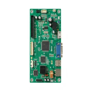
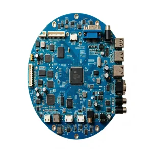

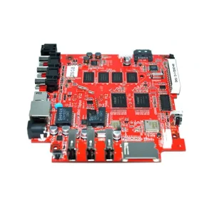
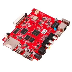
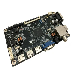
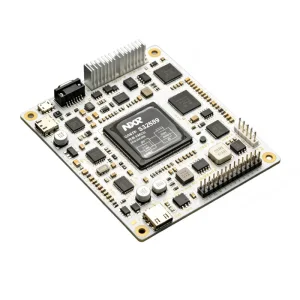

The printed circuit board assembly (PCBA) sector is navigating a momentous structural transformation. Rapid advancements in edge-computing artificial intelligence, wide-bandgap (WBG) semiconductors (Gallium Nitride and Silicon Carbide), and high-density automotive interconnects have made transactional electronics manufacturing obsolete. Today’s industrial, automotive, and medical enterprises require full-lifecycle EMS (Electronics Manufacturing Services) integration—where bare board fabrication, active bill-of-materials (BOM) optimization, micro-pitch surface-mount technology (SMT), automated firmware flashing, and full-enclosure box builds are merged under one audited, real-time traceable digital umbrella.
As component footprints condense toward ultra-fine packages such as 01005 passive chips, 0.3mm pitch Micro-BGAs, and Quad-Flat No-Leads (QFN), the tolerance margins in solder paste printing and reflow thermal stabilization have narrowed to single-digit microns. This evolution has redefined the criteria for evaluating qualified PCBA factories: automated inline solder paste inspection (SPI), multi-angle 3D Automated Optical Inspection (AOI), and non-destructive 3D Automated X-ray Inspection (AXI) are no longer premium options; they are non-negotiable operational requirements for eliminating latent solder bridging, head-in-pillow defects, and micro-voiding.
With the proliferation of 5G RF nodes, high-speed compute engines, and automotive power electronics, assemblies require advanced mixed-dielectric substrates (e.g., Rogers bonded to FR-4), heavy-copper inner layers up to 6oz, and precision thermal vias to channel thermal loads away from critical processing cores.
Industrial and medical form-factors demand High-Density Interconnect (HDI) structures with stacked microvias, laser direct imaging (LDI), and sub-0.35mm pitch CSP component arrays. Controlling solder volume deposition within ±5% volumetric variance is mandatory to avoid parasitic capacitance and crosstalk.
Modern original equipment manufacturers (OEMs) demand comprehensive item-level traceability. Every surface-mount component reel, paste batch lot, reflow thermal profile record, and functional board test result must be mapped to a machine-readable 2D Datamatrix barcode, guaranteeing instant forensic root-cause discovery.
How Shenzhen STHL Electronics leverages the world’s most concentrated hardware cluster to compress engineering turnaround times, eliminate single-source dependencies, and provide scalable manufacturing velocity.
Located in Bao'an District, Shenzhen—the epicenter of global electronics innovation—STHL synthesizes two decades of practical manufacturing know-how with the world’s fastest supply chain cluster. While regional competitors struggle with component lead-times exceeding 16 weeks, our direct API-level connections with over 100 franchised semiconductor distributors (including Arrow, Avnet, Digi-Key, Mouser, Farnell, and direct fab relationships with STMicroelectronics and Microchip) provide instant visibility across 500,000+ active part numbers.
This physical clustering allows STHL to complete prototype DFM revisions in under 24 hours, procure rare passive packages within 48 hours, and transition seamlessly from a 10-board prototype run to a 500,000-unit monthly mass production campaign on identical Panasonic and Yamaha high-speed pick-and-place lines. The result: zero requalification delays, absolute bill-of-materials integrity, and significant structural cost advantages passed directly to overseas enterprise buyers.
Our 50+ engineers scrutinize your BOM to identify obsolete, long-lead, or single-source components, proposing drop-in, pin-compatible alternates that reduce component acquisition costs by 15% to 35% without altering board layouts.
Integrated Manufacturing Execution Systems (MES) govern feeder placement verification, stencil solder viscosity, multi-zone reflow temperature telemetry, and post-assembly functional test parameters with automated line lockout controls.
We eliminate minimum order barriers. Design verification test (DVT) batches of 5 units receive the exact same engineering scrutiny, laser stencils, and optical profiling as 100,000-unit automotive high-volume production orders.
Rigorous Non-Disclosure Agreements (NDAs) are signed prior to CAD Gerber data exchange. Firmware binaries are flashed in segregated, air-gapped programming cells with encrypted hash verification to guarantee zero proprietary leakage.
How procurement teams, supply chain directors, and chief technology officers can eliminate vulnerabilities across quality, counterfeit components, and international logistics.
Suboptimal component spacing, uneven copper balances, or undersized thermal pads cause assembly line solder bridging and tombstones. STHL executes automated and manual DFM/DFA checks across 45 discrete layout checkpoints before issuing stencil orders, preventing costly engineering change orders (ECOs) post-fabrication.
The gray component market presents severe reliability risks. Our incoming material inspection protocol includes microscopic package de-capsulation checks, pin-oxidation testing, X-ray lead-frame analysis, and component serialization checks against authorized manufacturer batch databases to ensure 100% authentic active and passive silicon.
Low unit quotes often mask post-production costs from field returns, testing bottlenecks, and hidden freight markups. By providing transparent, line-item pricing across fabrication, parts, assembly, testing fixtures, and conformal coating, STHL lowers long-term operational expenditures across the complete product lifecycle.
Gerber, BOM, and centroid validation under NDA
Traceable procurement and incoming batch lab testing
Multi-layer HDI, impedance control, high-Tg base
Laser stencils, 10-zone reflow, dual-wave DIP
100% optical inspection and BGA micro-voiding analysis
Custom bed-of-nails, flashing, and burn-in aging
Enclosure integration, ESD vacuum sealed export
Our manufacturing operations adhere strictly to international quality and safety benchmarks, supported by rigorous audits across automotive, medical, and environmental standards.
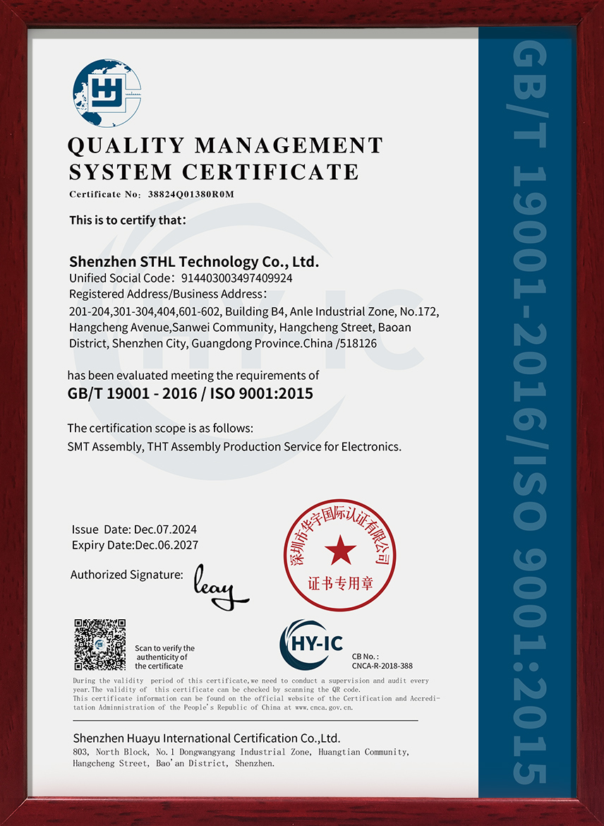
Comprehensive Quality Management System governing standard operating procedures, documentation, and continuous process improvements.
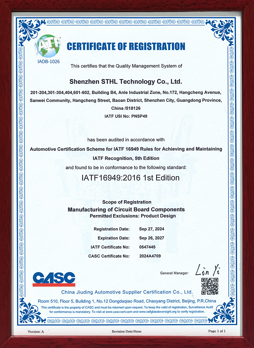
Global automotive electronic standard enforcing APQP, PPAP level 3 submissions, FMEA risk reduction, and zero-defect SMT placement.
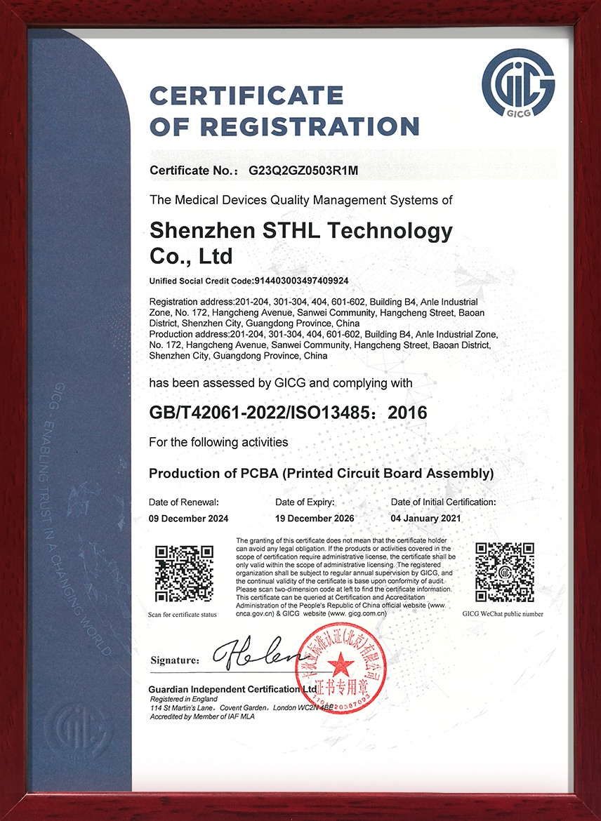
Medical device quality assurance system verifying traceability, cleanroom manufacturing controls, and device lifecycle validation.
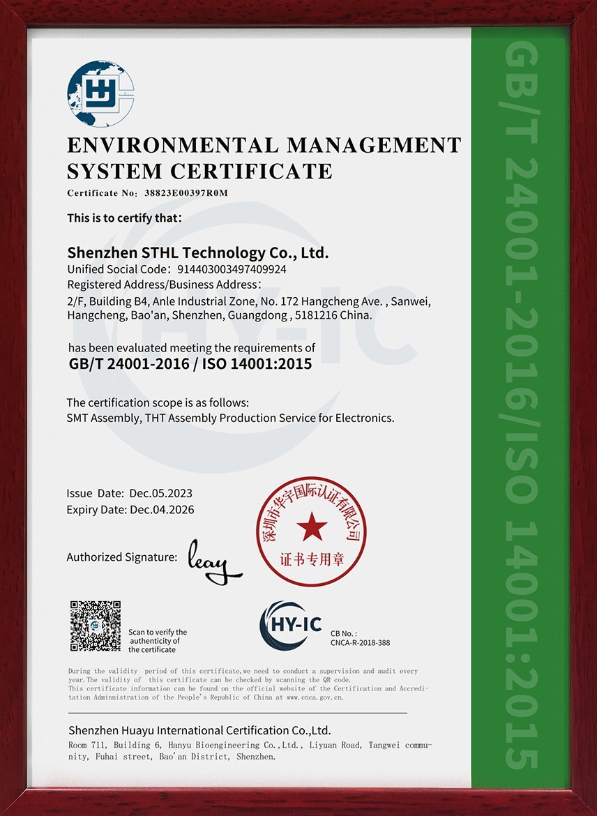
Environmental management standard guaranteeing RoHS 3, REACH, and lead-free (Pb-free) compliant solder waste treatment.
| SMT Component Footprint Range | Passives down to 01005 (0402 metric); active ICs up to 55mm × 55mm BGA, CSP, QFN, POP (Package-on-Package). |
|---|---|
| BGA Pitch & Ball Diameter | Minimum BGA Ball Pitch: 0.30mm (12 mil); Ball Diameter: 0.15mm; 100% 3D X-Ray verified for voiding < 15%. |
| Placement Accuracy & Speed | ±0.035mm (35µm) chip repeatability; high-speed automated placement capacity up to 120,000 components per hour per line. |
| Board Dimension Envelope | Min PCB Size: 50mm × 50mm; Max PCB Size: 610mm × 510mm; Board Thickness: 0.2mm to 4.5mm. |
| Substrate Chemistries | Standard FR-4, High-Tg (TG170/180), Halogen-Free, Flex (PI/PET), Rigid-Flex, Aluminum-Core Metal Backed, Rogers High-Freq, PTFE, Ceramic. |
| Soldering Capabilities | Lead-Free (SAC305, SAC0307) and Leaded (Sn63Pb37) reflow soldering; Nitrogen (N2) atmosphere capable; Selective wave soldering; Manual soldering per IPC-A-610 Class 3. |
| Value-Added Finishing Services | Automated conformal coating (acrylic, silicone, polyurethane), potting, laser engraving, IC flashing, cable harness fabrication, custom sheet metal/plastic enclosure box build. |
| Test Coverage & Verification | SPI, 3D AOI, 3D AXI (X-Ray), In-Circuit Testing (ICT), Flying Probe, Automated Functional Circuit Testing (FCT), Thermal Shock, Burn-in Chamber testing. |
From aerospace avionics and medical life-support devices to extreme-duty automotive powertrain modules and renewable energy grids, STHL boards are designed and assembled for demanding operating environments.
Operating under IATF 16949 standards, we produce Head-Up Display (HUD) boards, LiDAR sensors, battery management systems (BMS), and powertrain controllers engineered for continuous thermal cycling from -40°C to +125°C with zero solder fatigue.
Assembled within ISO 13485-certified cells, our medical assemblies power surgical navigation hardware, blood pressure telemetry systems, and ICU ventilators with Class 3 IPC-A-610 soldering standards and complete component traceability.
We supply high-efficiency power generation controllers, distributed wind-power inverters, particle air monitors, and smart environmental telemetry nodes built to withstand high EMI/RFI and outdoor operating conditions.
Challenge: A European medical equipment client experienced intermittent signal drift caused by 22% solder voiding in an FPGA 0.4mm pitch Micro-BGA package.
STHL Solution: Our engineering team restructured the stencil aperture from circular to a modified micro-square cross-hatch design, shifted from SAC305 to an ultra-low voiding Type 4 solder paste, and recalibrated the reflow profile to incorporate a 45-second nitrogen-inert soak at 180°C.
Outcome: Average solder voiding dropped below 7.2% across three production batches, eliminating field signal loss and accelerating the customer's CE-MDR medical device certification.
Our secondary portfolio showcases solutions for automotive HUD displays, green energy controllers, medical ventilators, benchtop lab power supplies, and industrial environmental analyzers.
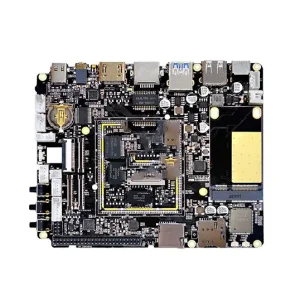
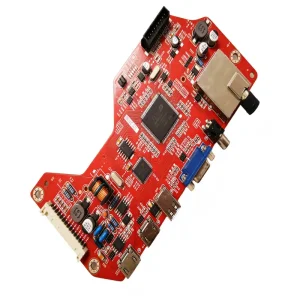


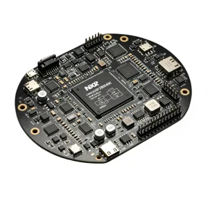
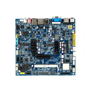

Verified testimonials from international technology companies and sourcing managers across North America, the European Union, South America, and the Asia-Pacific region.
"Excellent engineering collaboration, responsive DFM feedback, and fast turnaround on complex boards. STHL has proven to be an exceptional manufacturing partner for our US product line."

"Please extend my thanks to your engineering team for their diligent preparation of our pre-production pilot. The level of traceability gave us complete confidence to move into full-scale mass production."

"We were thoroughly impressed with the production velocity and clean solder finishes on our industrial controllers. The short lead time saved our rollout timeline in Italy."

Clear technical answers to help purchasing teams and design engineers qualify STHL as their long-term electronics assembly partner.
Join forward-thinking OEMs across the USA, Germany, Italy, the UK, and 90+ other countries. Share your Gerber data and Bill of Materials to receive an engineering DFM evaluation and transparent turnkey quote within 24 hours.
