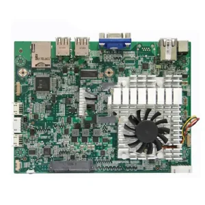
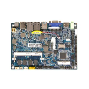
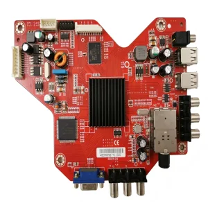
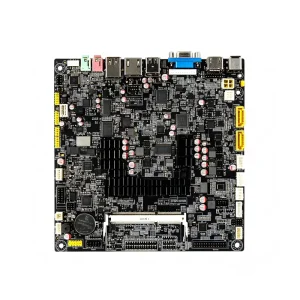
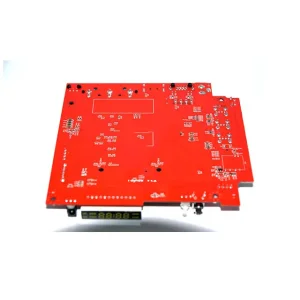
Engineered for mission-critical deployments across agricultural automation, industrial signage, edge sensing, and clinical informatics.
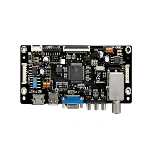
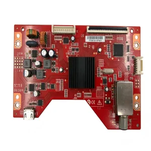
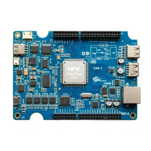
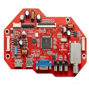
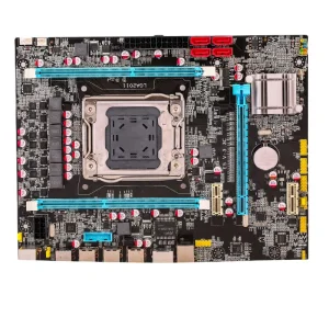
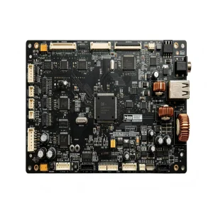
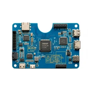
Demystifying signal integrity, thermomechanical laminate behavior, and structural defect mitigation in modern Bare PCB fabrication.
In the contemporary landscape of high-frequency switching, edge-computing intelligence, and miniaturized electromobility systems, the bare printed circuit board (Bare PCB) is no longer a passive substrate; it is an active, precision-engineered component of electromagnetic design. Selecting a bare PCB manufacturer requires evaluating critical variables across substrate physics, copper foil topology, automated chemical plating, dielectric breakdown margins, and structural impedance tolerances.
Modern printed circuit boards operate under severe thermomechanical strains. From high-voltage battery management systems (BMS) in automotive platforms requiring heavy-copper dissipation to aerospace-grade RF front-ends demanding ultra-low dielectric losses (Df < 0.002), the mechanical substrate dictates the final product's mean time between failures (MTBF). At STHL, bare PCB engineering encompasses rigorous substrate qualification, laser direct imaging (LDI), automated optical shaping, and multi-stage electrical testing (flying probe and dedicated universal grid fixture testing) to guarantee zero open, short, or latent micro-defects.
| Fabrication Parameter | Standard Commercial PCB | Advanced Industrial PCB | STHL Aerospace & Medical Grade |
|---|---|---|---|
| Layer Count Capability | 1 – 8 Layers | 10 – 24 Layers | Up to 48 Layers (Any-Layer HDI) |
| Minimum Trace / Space (L/S) | 100 / 100 µm (4/4 mil) | 75 / 75 µm (3/3 mil) | 35 / 35 µm (mSAP Sub-25µm) |
| Microvia Aspect Ratio | 0.8:1 | 1:1 (Stacked / Staggered) | 1.2:1 (Direct Laser Microvias) |
| Impedance Control Tolerance | ± 10% Standard | ± 7% Tight | ± 5% Polar CITS Precision |
| Base Laminates Supported | Standard FR-4 (Tg 130-140°C) | High-Tg FR-4 (Tg 170-180°C) | Rogers, Megtron 6/7, Polyimide, Al/Cu Core |
| Surface Finish Metallurgy | HASL / Lead-Free HASL | ENIG (Electroless Ni / Immersion Au) | ENEPIG, Immersion Ag, Hard Gold >30µ" |
| Quality Standards Compliance | IPC-A-600 Class 1 & 2 | IPC-6012 Class 2 / ISO 9001 | IPC-6012 Class 3 / 3A, IATF 16949, ISO 13485 |
Strategic advancements transitioning PCB manufacturing into the era of Substrate-Like PCBs (SLP), co-packaged optics, and ultra-high thermal dissipation.
Employing modified Semi-Additive Processes (mSAP) allows line widths down to 25/25 µm, bridging the gap between conventional PCB fabrication and advanced IC packaging. Vital for ultra-dense wearables and 5G/6G millimeter-wave RF modules.
Addressing the intense heat flux of silicon carbide (SiC) and gallium nitride (GaN) wide-bandgap semiconductors via embedded copper coin geometries, direct-bonded copper (DBC), and thick-film ceramic substrates.
Eliminating dielectric glass weave skew through spread-glass fabrics and proprietary resin systems (Dk < 3.2, Df < 0.0015). Engineered backplanes for artificial intelligence servers, optical transceiver routing, and radar transceivers.
Integrating passive capacitance and resistance directly within internal prepreg layers to reclaim up to 40% surface real estate, lowering parasitic inductances and enabling seamless transition to integrated photonics.
Tailoring dielectric chemistry, copper weight, and cleanliness compliance to the operational extremes of target operating environments.
Automotive electrification demands bare PCBs engineered to withstand harsh vibrations, wide operating temperatures (-40°C to +150°C), and transient high currents. We manufacture boards for Inverters, On-Board Chargers (OBC), and BMS systems with heavy copper (up to 12 oz) and verified Conductive Anodic Filament (CAF) resistance.
For patient-monitoring terminals, surgical imaging, and portable diagnostic analyzers, bare board integrity is life-critical. Our fabrication lines enforce strict bio-burden control, high-cleanliness ionic contamination limits (< 0.5 µg/cm² NaCl equivalent), and micro-via structural integrity validation under IPC Class 3.
High-voltage isolation, transient surge suppression, and continuous duty cycles require specialized thick dielectric margins, robust soldermask chemical resistance, and high Comparative Tracking Index (CTI > 600V) laminate selections to prevent surface tracking.
Combining automated chemical closed-loops, AI-driven process inspection, and Shenzhen's hyper-dense component ecosystem to mitigate global supply volatility.
Global procurement directors face unprecedented supply chain headwinds: fluctuating raw material prices, geopolitical customs bottlenecks, and volatility in copper foil availability. STHL’s smart manufacturing facility in Bao'an, Shenzhen counters these vulnerabilities through end-to-end digitisation and direct vertical integration.
By connecting Manufacturing Execution Systems (MES) directly to Enterprise Resource Planning (ERP) databases, every copper panel, dry film batch, chemical etchant replenishment, and automated optical inspection (AOI) record is synchronized to a unique panel serialization matrix. This eliminates human transcription drift and enables automated SPC (Statistical Process Control) alarm triggers before process deviations affect yield.
Direct supply contracts with top-tier laminate suppliers (Shengyi, Kingboard, Rogers, ITEQ) ensure priority access to raw copper-clad laminates (CCL) and chemical salts, reducing spot-market price volatility for overseas clients.
Seamless design migration from 24-hour rapid prototyping lines directly into high-speed automated mass-production panels without renegotiating stack-up chemistry or re-qualifying core drill parameters.
High-resolution Automated Optical Inspection (AOI) paired with deep-learning classification filters out false alarms and captures insidious defects like micro-voids, plating cracks, and mouse bites down to 5 µm.
From comprehensive Design for Manufacturability (DFM) audits to total cost of ownership (TCO) optimization and rigorous IP protection.
Over 80% of PCB assembly rework traces back to bare board layout defects. STHL’s dedicated engineering team evaluates Gerber, ODB++, and IPC-2581 data sets for solder mask slivers, acid traps, aspect ratio limits, and thermal relief balance before dry film exposure begins.
For international OEMs and enterprise hardware brands, technical files represent core competitive IP. STHL operates on encrypted internal air-gapped engineering networks with mandatory Non-Disclosure Agreements (NDAs) enforced prior to reviewing quote documentation.
Procurement is not merely unit pricing—it is minimizing scrap rates, avoiding field recall liabilities, and eliminating assembly downtime. Our bare boards guarantee maximum solderability and planarity, minimizing SMT misalignments and tombstoning.
Ensuring your hardware passes every regulatory hurdle across North American, European, and Asia-Pacific customs jurisdictions.
All fabricated boards are completely compliant with EU Directive 2011/65/EU (RoHS 2.0) and REACH (EC 1907/2006). Every batch is verified via XRF spectroscopy for heavy metal and flame retardant exclusions (lead, cadmium, mercury, PBB/PBDE).
STHL’s base materials and solder masks carry certified UL 94V-0 yellow cards, ensuring self-extinguishing flame retardant properties vital for consumer safety, industrial electrical cabinets, and telecommunications installations.
With an audited 99.5% on-time delivery metric, we coordinate turnkey DDP (Delivered Duty Paid), FOB, and DAP air/sea freight logistics across North America, Europe, South America, and APAC with full customs clearing management.
Detailed engineering responses answering the most common queries from procurement specialists, layout engineers, and quality auditors.
We perform pre-manufacturing impedance modeling using Polar Instruments Si9000e transmission line field solvers. During production, every production panel includes dedicated test coupons at the periphery. Coupons are validated using Time-Domain Reflectometry (TDR) to ensure single-ended (±5% or ±7%) and differential traces conform strictly to specifications.
IPC Class 3 mandates substantially stricter fabrication tolerances for mission-critical applications: minimum through-hole copper plating thickness of 25 µm (vs 20 µm in Class 2), zero copper annular ring breakout allowance (internal and external), and far more stringent ionic contamination thresholds to withstand continuous, uncompromising field operations.
Electroless Nickel Electroless Palladium Immersion Gold (ENEPIG) introduces a palladium barrier layer (0.05–0.15 µm) between the nickel and gold. ENEPIG completely prevents the "black pad" corrosion syndrome occasionally found in fine-pitch ENIG, offers superior multi-reflow thermal longevity, and allows both gold wire bonding and SAC solder joints on the same substrate.
Our centralized procurement office integrates direct API inventory feeds with authorized tier-1 distributors (Arrow, Avnet, Digi-Key, Mouser, Farnell) and direct franchise silicon fabricators. We offer real-time lifecycle tracking (EOL/NRND alerts) and provide pin-compatible drop-in alternate proposals during DFM review to ensure uninterrupted manufacturing schedules.
To provide an exact, engineering-validated quote within 24 hours, we require: Gerber files (RS-274X or ODB++ format), IPC-NC-349 drill files, layer stack-up definitions specifying target copper thickness, soldermask/silkscreen color, surface finish preference, and specific IPC Class or impedance requirements.
Yes. For RF and millimeter-wave modules requiring both digital processing and low-loss microwave performance, we routinely bond Rogers/PTFE high-frequency layers to high-Tg FR-4 digital backplanes. This hybrid laminate approach optimizes high-speed signal integrity while minimizing overall substrate costs.
Explore STHL's specialized PCBA capabilities delivering verified reliability across extreme environmental profiles.