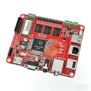
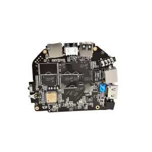
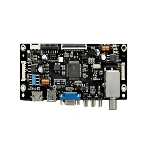
High-density surface mount and through-hole assemblies manufactured to rigorous automotive, aerospace, and medical specifications.
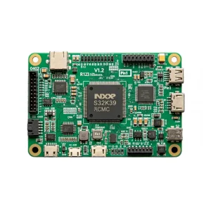
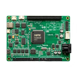
Navigating the transition toward miniaturized high-density packaging, 800V silicon-carbide mobility, and ultra-high-frequency substrate designs.
The accelerating demand for edge computing, artificial intelligence micro-servers, and ultra-compact medical implantable systems has forced a technological paradigm shift in circuit board parts factories. Traditional multi-layer FR-4 circuit structures with mechanical drill limits of 0.15 mm are rapidly being superseded by Substrate-Like PCBs (SLP) utilizing modified semi-additive processes (mSAP). These advanced fabrication technologies achieve line widths and line spacings (L/S) below 25/25 μm, enabling direct integration of 0.3 mm pitch fine-pitch ball grid arrays (FPBGA) and ultra-miniature 01005 (0402 metric) passive discrete parts.
State-of-the-art circuit board manufacturing plants are increasingly executing multi-tier microvia architectures—including stacked and staggered laser microvias filled with electroplated copper (VIPPO - Via-in-Pad Plated Over). This architectural enhancement dramatically reduces parasitic inductance and signal reflection, preserving signal integrity across high-speed digital buses operating beyond 112 Gbps PAM4.
With the automotive transition from 400V battery architectures to 800V Silicon Carbide (SiC) and Gallium Nitride (GaN) wide-bandgap powertrains, thermal density management within electronic control units (ECUs) and power inversion circuits has escalated into a pivotal qualification metric. Contemporary circuit board factories must engineer specialized metal-core boards (MCPCB), heavy-copper substrates (exceeding 4 oz to 10 oz copper thickness), and ceramic substrates (AlN - Aluminum Nitride, Al2O3 - Alumina) possessing thermal conductivities reaching 170–200 W/m·K.
Furthermore, high-voltage galvanic isolation compliant with IEC 60664-1 requires specialized comparative tracking index (CTI ≥ 600V, Material Group I) resin chemistries to inhibit electrochemical dendritic migration under continuous high-thermal and high-humidity environmental stresses.
Integration of Rogers RO4350B, RO3003, and Panasonic Megtron 6/7 dielectrics with standard FR-4 to optimize insertion losses in 77GHz automotive radar and satellite payloads.
Elimination of conventional wiring harnesses through dynamically flexible polyimide (PI) circuits with adhesiveless copper, reducing mass by up to 60% while mitigating physical vibration disconnects.
Automated selective robotic dispensing of Parylene, silicone, and polyurethane elastomeric barriers to shield bare circuits and solder fillets from salt spray, fuel vapors, and conductive dust.
Procurement executives demand comprehensive transparency, lifecycle obsolescence hedging, and certified anti-counterfeiting protocols.
In an era punctuated by geopolitical supply disruptions and component allocation bottlenecks, global Original Equipment Manufacturers (OEMs) can no longer rely on unverified brokers. Sourcing departments partner with world-class circuit board parts factories that implement strict AS6081 and AS6171 standardized testing to detect cloned, re-marked, or refurbished silicon before reels reach the pick-and-place feeders.
At STHL Electronics, incoming electronic components are subjected to heated chemical solvent tests, fine and gross leak hermetic checks, internal visual decapsulation (die verification), and high-resolution automated X-ray fluorescence (XRF) spectroscopy to authenticate lead finishes and RoHS elemental compliance.
| Manufacturing Parameter | Standard Capability | Advanced / High-Density Capability | Compliance / Verification Standard |
|---|---|---|---|
| Layer Count | 1 to 16 Layers | Up to 48 Layers (Multi-layer Rigid / HDI) | IPC-6012 Class 2 / Class 3 |
| Min. Line Width / Spacing | 3.5 mil / 3.5 mil (90 μm) | 2.0 mil / 2.0 mil (50 μm) with mSAP | AOI Laser Micrometer Inspection |
| SMT Placement Pitch | 0402 metric / 0.5 mm BGA pitch | 01005 metric / 0.3 mm Ultra-Fine Pitch CSP | 3D SPI + 3D AOI (Koh Young) |
| Microvia / Blind Via Diameter | 0.15 mm (Mechanical Drill) | 0.075 mm (UV / CO2 Laser Drilling) | Micro-section Cross-Sectioning |
| Impedance Tolerance | ± 10% Controlled Single / Diff | ± 5% Polar CITS880s TDR Testing | IPC-2141 Design Guidelines |
| Surface Finishes | HASL, Lead-Free HASL, OSP | ENIG, ENEPIG, Immersion Silver/Tin, Hard Gold | IPC-4552 / IPC-4556 Standards |
From safety-critical automotive ECUs to implantable Class III medical electronics, discover our cross-domain engineering frameworks.
Fabricated within IATF 16949 certified workshops. Rigorous PPAP Level 3 documentation, FMEA defect analysis, and 100% boundary scan testing for powertrain controls, battery management systems (BMS), and ADAS sensing radars.
ISO 13485 certified cleanroom assembly for clinical physiological monitors, diagnostic imaging motherboards, and life-supporting pacemaker subassemblies. Full DHR (Device History Record) archival and bio-burden controls.
Built to IPC-A-610 Class 3 specifications with automated conformal barrier application. Engineered for flight-critical air data computers (ADCs), harsh vibration dampening, and vacuum outgassing resilience under ASTM E595 standards.
Ruggedized programmable logic controller (PLC) and particle monitor circuit boards with high surge suppression, thermal cycling durability from -40°C to +125°C, and conformal potting against corrosive gaseous environments.
Quantifiable manufacturing capacity delivering rapid-turn prototyping through multi-million unit scalable batch production.
Eliminating international procurement risk with rigorous quality management certifications and comprehensive MES data capture.
STHL operates strict, audited management systems certified to IATF 16949 (Automotive), ISO 13485 (Medical Devices), ISO 9001 (Quality Management), and ISO 14001 (Environmental Stewardship), ensuring uncompromising process consistency across every production run.
Barcoded 2D matrix laser labeling on each printed circuit board locks complete component reel ID, reflow thermal profile history, SMT machine telemetry, and AOI inspection images into permanent cloud archives for flawless 10-year auditability.
Fully compliant with EU RoHS 3 (Directive 2015/863) and REACH SVHC regulations. Conflict Mineral reporting templates (CMRT) provided. Direct door-to-door DDP air freight coverage across North America, Europe, Australia, and APAC.
Engineering readiness for System-in-Package (SiP), cryogenic computing, and AI-driven predictive process control.
As physical printed circuit board footprint constraints tighten in next-generation medical wearables and military avionics, conventional surface component soldering hits its geometric limit. Our engineering roadmap integrates active silicon dies and passive discrete resistors/capacitors embedded directly into inner laminate prepreg cores. This inner-layer burial minimizes loop inductance to sub-nanohenry levels while freeing outer layers for ultra-dense sensor arrays and heat-spreading copper pours.
Moving beyond conventional rule-based 2D optical inspection, our production floor utilizes deep-learning neural networks trained on millions of solder fillet topologies. The AI engine classifies micro-voiding within BGA solder spheres (keeping voiding below 10%, well beneath the IPC 25% threshold), detects head-in-pillow (HiP) anomalies in real-time, and continuously adjusts reflow oven convection zone temperatures to maintain solder viscosity equilibrium.
Explore additional domain-engineered turnkey circuit assemblies built by Shenzhen STHL Electronics.
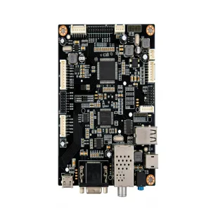
Addressing the critical evaluation questions hardware designers and supply chain executives present during factory audits.
Connect directly with STHL's senior hardware engineers to optimize your circuit board parts bill-of-materials, analyze fabrication stack-ups, and receive competitive turnkey PCBA quotations.
Connect With Engineering