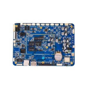
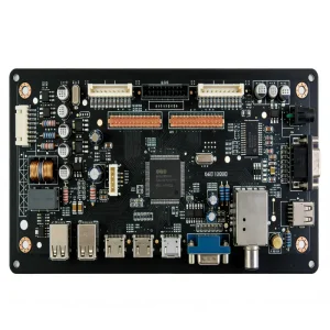
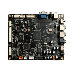
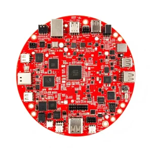
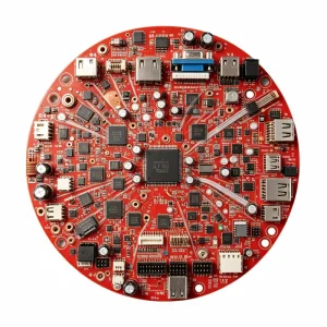
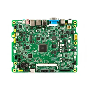
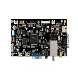
High-yield SMT, THT, and electromechanical box builds engineered under automated pick-and-place lines, nitrogen-inert reflow tunnels, and 3D automated inspection protocols.

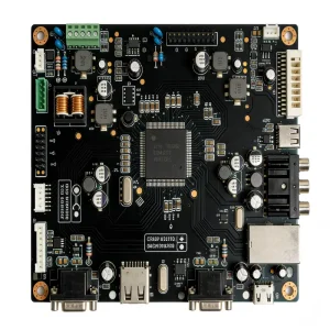
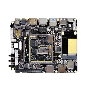
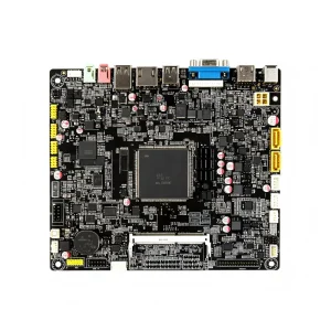

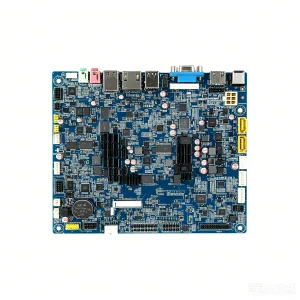
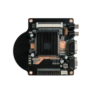
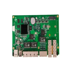
The paradigm of global electronics manufacturing is undergoing an aggressive technological reset. Modern high-quality electronic assembly equipment factories are transforming from manual fabrication hubs into hyper-automated cyber-physical ecosystems.
Modern electronic assembly machinery operates at placement cadences surpassing 100,000 components per hour (CPH) with positional accuracies down to ±15 microns. Achieving zero coplanarity error on ultra-fine-pitch 01005 passives and 0.3mm ball-grid arrays (BGAs) demands closed-loop dynamic machine vision, rotary placement head stabilization, and linear motor drive technologies.
Over 65% of surface-mount assembly defects originate during solder paste printing. Premier electronic assembly equipment factories now enforce true closed-loop communication between high-precision stencil printers and inline 3D Solder Paste Inspection (3D-SPI) systems, automatically adjusting stencil aperture alignment and squeegee pressure in real time.
Transitioning to SAC305 and ultra-low-voiding lead-free solder pastes requires multi-zone reflow convection ovens equipped with pure nitrogen (N2) shielding. Maintaining oxygen levels below 500 PPM prevents terminal oxidation, minimizes intermetallic compound (IMC) thickness, and eliminates wetting de-wetting micro-failures on critical safety boards.
Splitting PCB fabrication, passive component procurement, surface-mount placement, and electromechanical box building across fragmented subcontractors introduces fatal blind spots in quality traceability and lifecycle longevity. Leading OEMs now partner exclusively with single-source electronic manufacturing facilities executing comprehensive ERP and MES machine telemetry.
Institutionalizing aerospace, medical, and automotive-grade reliability across 10,000+ square meters of cleanroom production space in Bao'an, Shenzhen.
How artificial intelligence, optical telemetry, robotic material logistics, and predictive failure analysis are reshaping surface-mount production lines worldwide.
Traditional rule-based AOI suffers from false-call rates exceeding 15%. Integrated neural networks trained on millions of soldering joints now differentiate non-critical cosmetic variations from true defects such as micro-bridging, tombstoning, and lifted leads.
Autonomous material handling carts interface directly with component reel carousels and pick-and-place feeder docks. Automated reels with RFID and laser barcoding verify lot codes before loading, completely mitigating component mix-up human errors.
Intelligent motor-driven micro-feeders compensate dynamically for tape pocket vibration and pitch inconsistencies. Pitch indexing happens in milliseconds, ensuring high-speed continuous feeding without tape jamming or high-value component attrition.
By monitoring spindle temperature, vibration frequency, and vacuum nozzle pressure drop, central factory AI predicts suction cup wear or axis degradation hours before mechanical breakdown, safeguarding 99.8% equipment availability.
Rigorous engineering benchmarks powering STHL's 7 high-speed SMT lines, dual wave-soldering lines, and dedicated functional testing suites in Shenzhen.
| Equipment / Process Dimension | Standard Industry Threshold | STHL Factory Advanced Capability | Compliance & Verification Method |
|---|---|---|---|
| Min. Passive Component Size | 0402 Metric / 0201 Imperial | 01005 (0.4 × 0.2mm) & 008004 Capable | Closed-loop 3D AOI Verified |
| BGA & CSP Ball Pitch | 0.50 mm (19.7 mil) | 0.30 mm Ultra-Fine Pitch CSP / BGA | 3D AXI X-Ray Void Ratio <8% |
| SMT Placement Repeatability | ±35 microns @ 3 Sigma | ±15 microns @ 3 Sigma (High-Res Vision) | Laser & Optical Glass Calibrated |
| Max Board Dimension | 450 × 350 mm | 650 × 500 mm (Oversized Backplanes & LED) | Multi-Stage Edge Clamping |
| Solder Paste Printing Accuracy | ±25 microns | ±10 microns (Fully Automatic Vision Stencil) | Real-Time In-line 3D SPI |
| PCB Substrate Versatility | Standard Rigid FR-4 only | Rigid-Flex, Polyimide, Rogers, Aluminum, Ceramic | Vacuum Supported Fixtures |
| Soldering Atmospheric Environment | Ambient Atmospheric Air | 10-Zone Forced Convection + Pure Nitrogen (N2) | Residual O2 < 500 PPM Monitored |
| Through-Hole Soldering Technique | Standard Manual Soldering Iron | Selective Soldering + Dual Nitrogen Wave Tunnel | IPC-A-610 Class 3 Meniscus Check |
Strategic horizon charting equipment miniaturization, advanced heterogeneous SiP packaging, digital-twin line simulations, and decarbonized manufacturing.
Engineered to meet the exact compliance criteria of Tier-1 industrial, medical, automotive, energy, and telecom engineering teams worldwide.
Automotive assemblies require zero-defect manufacturing under extreme vibration and temperature cycles (-40°C to +150°C). We deploy automated selective soldering, automated conformal coating with precise film-thickness verification, and 100% in-circuit stress screening.
Biomedical electronics demand full component traceability down to individual wafer lots. STHL implements laser serialization on every PCB panel, automated component verification, and rigorous ion chromatography tests to ensure ionic cleanliness surpasses IPC Class 3 limits.
Energy storage controllers and high-voltage DC-DC converters carry heavy copper layers (up to 6 oz) prone to thermal sink defects during reflow. Our multi-zone nitrogen ovens feature programmable bottom-side heaters to ensure flawless solder fillet formation without delaminating inner traces.
Bluetooth modules, environmental particle monitors, and soil detectors require low-noise ground loops and precise impedance control. We verify RF matching networks via high-frequency spectrum analyzers and execute automated functional RF shielding tests inside customized Faraday cages.
Rack-mounted power units and optical network terminals require sustained 24/7/365 operational stability under ambient dust and fluctuating electrical grids. Assemblies receive custom conformal potting, boundary-scan testing, and extended burn-in testing under full load.
Beyond the bare PCBA, we bridge electronic assembly equipment directly into finished product realization. Automated wire harness routing, ultrasonic plastic welding, precision CNC milling for enclosures, and custom retail packaging ensure seamless time-to-market.
Examining real-world production engineering challenges resolved through precision equipment calibration, thermal modeling, and custom automated fixtures.
Challenge: An energy client experienced intermittent solder bridge faults on 100A MOSFET thermal pads coupled with micro-voiding over 22%.
Solution: STHL engineering redesigned the stencil using nanocoated electroformed nickel apertures with a window-pane aperture pattern. We deployed a 10-zone nitrogen reflow profile with peak soaking at 242°C, shrinking solder void ratios below 6.8% and passing 1,000 thermal shock cycles (-40°C / +125°C).
Challenge: Soil detector microcontroller boards suffered dendritic growth and leakage currents when deployed in acidic, high-moisture agricultural soils.
Solution: Implemented automated robotic selective silicone conformal coating (IPC-CC-830 certified) with automated optical fluorescence inspection, guaranteeing uniform 50-micron coverage across high-impedance analog trace inputs.
Challenge: A German OEM experienced head-in-pillow (HiP) defects on 0.4mm pitch processor BGAs on a 12-layer high-Tg FR-4 network controller board.
Solution: Real-time dynamic warpage profiling using optical shadow moiré analysis during reflow heating. Adjusted flux chemistry to high-activity tacky gel flux and utilized inline 3D X-ray laminography, driving assembly first-pass yields from 88.4% to 99.8%.
Quality is never tested into a board—it is engineered into every stage of the cyber-physical process flow. Review our end-to-end defect prevention checkpoints.
X-ray fluorescence (XRF) material composition verification, moisture-sensitive level (MSL) baking chambers, and solderability dipping checks on all active and passive lots.
Moire phase-shift profilometry inspects 100% of solder deposits for volumetric accuracy, aperture bridge detection, and coplanarity before component placement begins.
Multi-angle telecentric cameras verify component presence, rotational shift, polarity alignment, tombstoning, and solder meniscus wetting against IPC-A-610 standards.
Computed laminography penetrates BGA balls, QFN sink pads, and press-fit connectors to quantify internal voids, accompanied by bed-of-nails functional firmware testing.
Essential technical checkpoints sourcing managers, procurement directors, and hardware engineers must verify before committing production tooling.
Does the factory maintain live MES data logging? Qualified facilities like STHL correlate individual PCB 2D DataMatrix codes with feeder reel lot numbers, reflow oven thermal records, SPI profiles, and operator IDs for at least 10 years of audit retention.
A premier assembly partner doesn't merely run Gerbers—they actively optimize them. Look for dedicated DFM/DFA engineers reviewing shadow effects on wave soldering, component spacing for automated pick-and-place nozzles, and fiducial marker clearance.
Ensure your contract manufacturer signs an enforceable Non-Disclosure Agreement (NDA) before file transmission, utilizes isolated air-gapped programming servers for encrypted hex files, and provides strict physically partitioned test facilities.
Direct, actionable answers to the key operational, technical, and logistical questions hardware founders and enterprise procurement leads ask STHL.
STHL covers the entire electronics manufacturing services (EMS) value chain: schematic/PCB layout review, global component sourcing via authorized franchises (Arrow, Digi-Key, Mouser, Avnet), bare PCB fabrication, high-speed SMT assembly, through-hole (THT) wave and selective soldering, BGA mounting, IC flashing, conformal coating, cable harnessing, box build assembly, and full functional testing.
No. STHL operates an agile manufacturing model with zero MOQ constraints. We support initial engineering prototype batches (5 to 50 units), low-to-medium pilot runs (100 to 2,000 units), and massive multi-million-unit mass production across our 7 automated SMT lines without requiring line re-qualification.
Our 10,000+ m² facility is certified under IATF 16949 (automotive defect prevention), ISO 13485 (medical equipment quality systems), ISO 9001 (general manufacturing quality), and ISO 14001 (environmental management). All operators and inspection engineers are certified to IPC-A-610 Class 2 and Class 3 workmanship criteria.
We purchase directly from original component manufacturers (OCM) and franchised global distributors. Every inbound passive, discrete, and IC package undergoes strict incoming inspection including decapsulation checks, XRF lead composition verification, pin solderability tests, and full MES barcode batch tracking.
To provide a fully verified turnkey quote within 24 to 48 hours, our engineering team requires: Gerber files (RS-274X or ODB++), complete Bill of Materials (BOM) detailing manufacturer part numbers and approved alternates, pick-and-place centroid coordinates (X, Y, rotation, layer), assembly drawings, and functional testing specifications.
We sign formal bilingual Non-Disclosure Agreements (NDAs) prior to receiving proprietary engineering documentation. Firmware flashing operates over encrypted, isolated local networks, ensuring binary images are never accessible via external internet links or unauthorized personnel.
Precision-engineered PCB assemblies, sensor controllers, power electronics, and industrial communication systems manufactured at STHL's high-tech Bao'an facilities.