
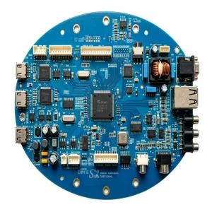
Explore our high-reliability PCBA assemblies deployed across enterprise computing, mission-critical acoustics, industrial power topologies, and automated electric transit solutions.
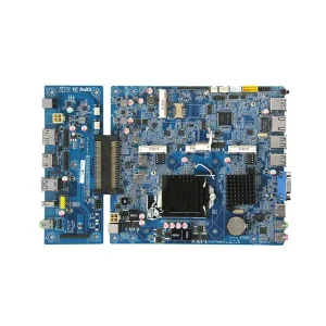
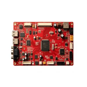
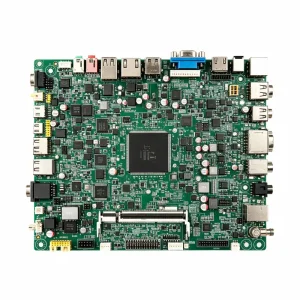
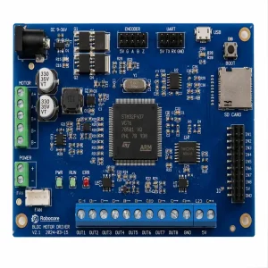
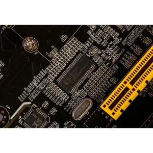

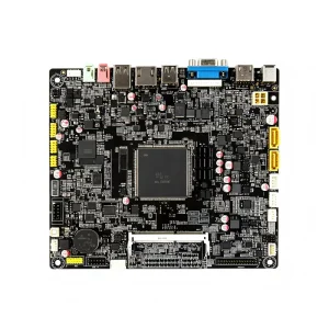
Why Tier-1 global technology leaders and high-growth hardware innovators continuously centralize their complex electronics manufacturing operations within Shenzhen's industrial cluster.
In the contemporary hardware landscape, the procurement of High-Quality Electronic Manufacturing Services (EMS) transcends simple contract labor arbitrage. Global OEMs operating across medical diagnostics, autonomous industrial machinery, advanced robotics, and mission-critical telecommunications require integrated ecosystems that merge high-mix low-to-medium volume (HMLV) agility with ultra-precision mass fabrication. The Greater Bay Area of China—specifically Shenzhen—remains the uncontested epicentre of global electronic manufacturing infrastructure, providing distinct supply chain compression that cannot be replicated elsewhere.
Within Shenzhen's Bao'an industrial corridors, an electronic engineering team can orchestrate prototype bare-board PCB fabrication, procure hard-to-find active semiconductors via authorized franchise distributors (Arrow, Avnet, Digi-Key, Mouser), execute custom CNC aluminum tooling, and conduct high-speed SMT assembly in a continuous 72-hour design cycle. This localized hyper-concentration of suppliers eliminates long maritime transit lead times during early revision stages, mitigating critical engineering change order (ECO) risks before initiating production ramp-up.
Furthermore, China's modern tier-1 electronic manufacturing factories have transitioned into digitalized, Industry 4.0 smart facilities. The historical dependence on manual labor has been superseded by high-precision Fuji, Yamaha, and Panasonic multi-function surface-mount mounters capable of 01005 passive placement, ultra-fine 0.3mm pitch micro-BGAs, automated 3D Solder Paste Inspection (SPI), high-speed 3D Automated Optical Inspection (AOI), and in-line X-ray tomography. As an IATF 16949 and ISO 13485 certified manufacturer, STHL PCBA exemplifies this technological modernization, managing every project through integrated ERP (Enterprise Resource Planning) and MES (Manufacturing Execution System) architectures that offer end-to-end component traceability down to individual reel barcodes and reflow thermal profile records.
Consolidated execution from PCB layout review, localized bare-board fabrication (FR4, HDI, Metal Core, Ceramic, Rigid-Flex), component procurement through 100+ vetted distributors, to turnkey box build.
Over 50 dedicated R&D and industrial engineers performing comprehensive Design for Manufacturability (DFM) and Design for Assembly (DFA) audits prior to surface-mount stencil fabrication.
Strict operational compliance across international quality systems: ISO 9001 (General Quality), ISO 13485 (Medical Systems), IATF 16949 (Automotive Zero-Defect), and ISO 14001 (Environmental Safety).
Navigating the major technological shifts defining the electronics contract manufacturing paradigm through 2030 and beyond.
The convergence of edge AI compute, autonomous robotics, wearable biomedical sensors, and distributed IoT nodes demands unprecedented component packing densities. Modern electronic manufacturing factories must consistently handle substrate designs featuring micro-vias down to 0.075mm, blind and buried via structures, 3-mil trace/space parameters, and package-on-package (PoP) assemblies. SMT lines require tight placement accuracy (±0.025mm at 3-sigma) to prevent bridging, tombstoning, or solder voiding under large ground pads.
RoHS and REACH compliance mandate specialized SAC305 (Sn96.5Ag3.0Cu0.5) and low-temperature bismuth-tin alloys. Because lead-free assembly operates at elevated liquidus temperatures (217°C compared to 183°C for traditional SnPb), strict 10-zone nitrogen-purged reflow ovens are utilized to maintain Delta-T across the entire PCBA below 5°C. This prevents catastrophic thermal stress on sensitive active microcontrollers, ceramic capacitors, and multilayer substrates.
Automotive electronics (IATF 16949) and Class II/III medical devices (ISO 13485) require absolute accountability. If a component fails in the field, manufacturers must isolate the exact PCB panel number, component date code, stencil lot, pick-and-place nozzle telemetry, and functional test record within minutes. STHL achieves this through individual 2D DataMatrix laser marking directly etched onto the bare circuit board before the initial solder paste application.
High-reliability PCBA solutions for EV battery management systems (BMS), motor control inverters, onboard infotainment head units, and telemetry gateway devices with high vibration resistance.
ISO 13485 validated cleanroom production for clinical noise analyzers, electronic medical record terminals, diagnostic monitors, infusion pump controllers, and patient-monitoring wearables.
High-efficiency DC-DC step-down converters, step-up boost controllers, smart commercial fire detection sensors, LoRaWAN gateways, and harsh-environment telemetry electronics.
A systematic comparison between working with an integrated direct PCBA manufacturer and utilizing third-party assembly middlemen or uncertified workshops.
| Evaluation Parameter | Certified Turnkey Factory (STHL PCBA Model) | Traditional Broker / Low-Cost Workshop |
|---|---|---|
| Direct Engineering Review | Formal DFM/DFA report generated prior to quoting; solder pad optimization, component clearance check, and stencil aperture engineering. | Basic quotation without mechanical or thermal scrutiny; design errors identified only after production floor halt. |
| Component Traceability | 100% Franchise Sourced directly through authorized distributors (Arrow, Avnet, Mouser) with full CoC documentation and MES reel tracking. | Frequent gray market procurement to optimize margin; heightened vulnerability to counterfeit or remarked ICs. |
| Quality Certification Stack | Audited Standards: IATF 16949 (Automotive), ISO 13485 (Medical), ISO 9001 (Quality), and ISO 14001 (Environmental). | Uncertified or self-declared ISO 9001 without valid third-party oversight; no process capability studies (Cpk ≥ 1.33). |
| Testing & Inspection Breadth | Multi-Gate Inspection: 3D SPI, 3D AOI (pre/post reflow), In-line High-Def X-Ray, In-Circuit Testing (ICT), and full Custom FCT. | Visual manual magnifying glass inspection only; basic power-on check with high field failure rate. |
| Intellectual Property Safeguards | Legally Binding NDA executed prior to receiving Gerber or BOM files; secure air-gapped programming servers. | Informal agreements; Gerber and firmware files circulated freely across unvetted subcontractors. |
| MOQ & Scalability Flexibility | Zero MOQ Barrier: Seamless transition from 5-piece engineering prototypes to 100,000+ unit mass production. | Rigid minimum order quantity restrictions or unwillingness to support low-volume validation iterations. |
A transparent, milestone-driven electronics manufacturing roadmap designed to eliminate engineering ambiguity and deliver zero-defect PCBA hardware.
Our senior hardware team inspects Gerber RS-274X/ODB++ files, validates footprints against IPC-7351 guidelines, and flags obsolete (EOL) components with form-fit-function alternatives.
Components are procured via authorized channels. Passive reels, silicon wafers, and electro-mechanical parts undergo incoming quality control (IQC) and moisture sensitivity packaging audits.
Bare printed circuit boards are fabricated to precise impedance parameters, controlled dielectric layers, and surface finishes (ENIG, Immersion Silver, OSP, or ENEPIG) with 100% Flying Probe verification.
Laser-cut electropolished stencils apply lead-free paste. Inline 3D SPI evaluates volume, area, and height before automated placement of micro-components and complex BGAs.
Multizone nitrogen reflow soldering follows custom thermal curves. Through-hole components are soldered using automated selective soldering or lead-free wave soldering with dedicated pallets.
Post-reflow inspection utilizes high-resolution 3D AOI for coplanarity and bridging. Hidden solder joints beneath BGA, QFN, and LGA packages undergo High-Resolution X-Ray Inspection (AXI).
Conformal coating (silicone, polyurethane, or acrylic) is applied for harsh-environment protection. Includes automated microcontroller firmware flashing, wire harness crimping, and box build integration.
Functional Circuit Testing (FCT) validates real-world voltage, current, and RF signal outputs. Approved units are vacuum-sealed in ESD bags, barcoded, and air-freighted globally with 99.5% on-time reliability.
Authoritative, engineering-level answers to critical technical and commercial questions raised by international procurement managers and hardware design directors.
Explore further assemblies covering intelligent medical records, automotive infotainment, wireless IoT infrastructure, commercial safety devices, and high-precision robotic controllers.
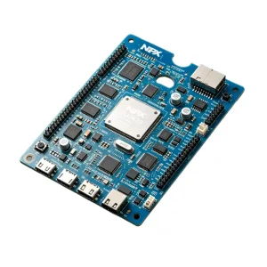
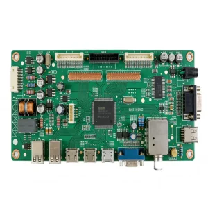
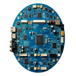
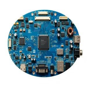
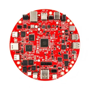
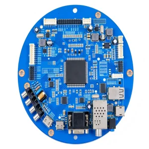
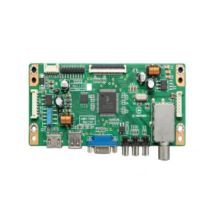
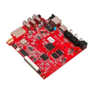
Verified manufacturing envelope parameters maintained across our Bao'an, Shenzhen smart production facility.
Minimum component pitch of 0.3mm for ultra-fine BGAs, micro-QFN, and LGA packages. Down to 01005 (0402 metric) passive chip components with high precision alignment.
Panel handling from 50mm × 50mm up to 610mm × 1200mm (large form factor LED and backplanes). Layer counts up to 32 layers with microvia structures.
Full inline coverage: 3D SPI, dual 3D AOI, high-magnification offline 3D X-Ray, In-Circuit Testing (ICT), Boundary Scan, and dedicated custom functional fixtures (FCT).
Procuring High-Quality Electronic Manufacturing r Factories & Factory partnerships is an investment in your product's lifecycle viability, market reputation, and commercial profitability. In an era punctuated by unpredictable supply chains, rapid silicon transitions, and tightening regulatory mandates, partnering with an accountable, certified, and digitally unified manufacturer in China ensures your hardware designs transition smoothly from initial Gerber validation to scalable market deployment. STHL PCBA continues to stand at the intersection of engineering discipline, technical innovation, and dependable electronics contract manufacturing for customers worldwide.