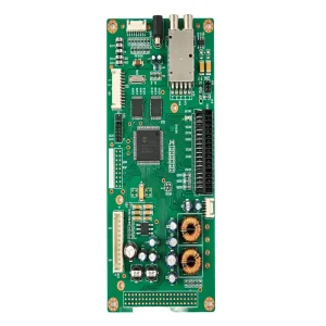
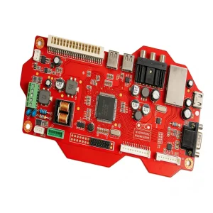
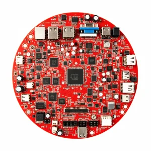
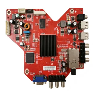
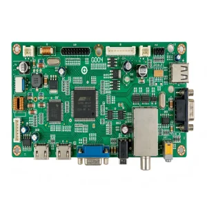
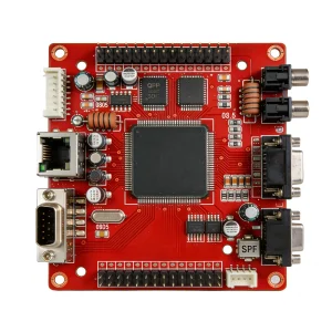
Engineered under IPC-A-610 Class 3 and automotive IATF 16949 standards, delivering verified zero-defect assemblies directly to worldwide OEM product lines.
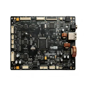
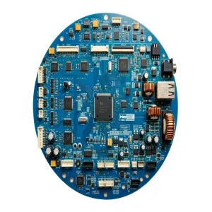
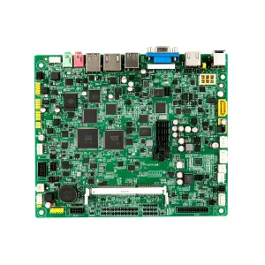
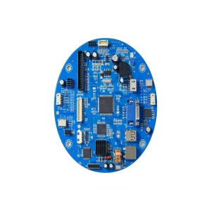
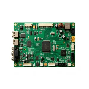
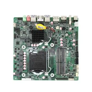


Analyzing procurement shifts, Total Cost of Ownership (TCO) variables, and how high-tier contract manufacturers reconcile agility with zero-defect quality.
The contemporary electronics contract manufacturing (ECM) ecosystem is experiencing a profound paradigm shift. As edge computing architectures, electromobility subsystems, and mission-critical medical diagnostics proliferate, global OEMs face escalating complexity. Designing a state-of-the-art circuit is no longer the sole bottleneck; rather, the enterprise's viability hinges on establishing an agile, dependable, and defect-free Electronics Manufacturing Services (EMS) partnership. High-reliability manufacturing requires navigating component volatility, evolving environmental compliance frameworks, micro-pitch component packaging, and stringent thermal dissipation thresholds.
Historically, contract electronics manufacturing was approached as a transactional, low-cost assembly exercise. Today, OEMs recognize that superficial unit cost is an incomplete and risky metric. The modern evaluation matrix focuses strictly on Total Cost of Ownership (TCO). Unbudgeted expenses caused by solder bridge bridging on 0.3mm pitch BGAs, undetected cold solder joints under thermal fatigue, unvetted semiconductor substitutions, and prolonged border clearance will instantaneously wipe out hypothetical margin gains achieved through bargain assembly shops. STHL addresses this macro challenge by bridging the gap between rigorous German/US engineering quality benchmarks and high-velocity Shenzhen ecosystem execution.
Factoring early-stage DFM feedback, component obsolescence hedging, automated ICT/FCT yields, and reduced warranty claims into a transparent, predictable manufacturing cost model.
Operating under certified IATF 16949, ISO 13485, and ISO 9001 quality regimes. Every single process gate utilizes closed-loop statistical process control (SPC) and real-time MES logging.
Seamlessly bridging quick-turn functional prototypes with mass-scale automated SMT lines. Zero redesign friction when transitioning from 5-piece pilot validation to 500,000-piece production.
Leveraging Shenzhen's Greater Bay Area industrial infrastructure to compress hardware delivery cycles and de-risk bill of materials procurement.
Shenzhen, China remains the uncontested epicenter of world-class electronics hardware innovation. Within a 30-kilometer radius of our Bao'an manufacturing center lies the world’s densest concentration of silicon distributors, passive component fabricators, precision toolmakers, bare laminate chemical specialists, and packaging pioneers. While western or regionalized EMS facilities frequently face 6-to-12-week lead times for passive re-spools or mechanical enclosure alterations, our centralized Greater Bay Area footprint enables same-day component dispatch, 24-hour rapid PCB laser tooling, and on-demand engineering collaboration.
Supply chain resilience at STHL is not an abstract aspiration; it is an active algorithmic process. Our central ERP system interfaces directly with over 100 franchised tier-1 global distributors—including Arrow, Avnet, DigiKey, Mouser, and verified original semiconductor fabricators—tracking more than 500,000 live part numbers. In scenarios where geopolitical volatility or sudden component allocations threaten an OEM's delivery schedule, our in-house team of 50+ senior component engineers immediately activates our second-sourcing qualification matrix: conducting parametric equivalence matching, thermal modeling, pin-to-pin footprint validation, and accelerated sample testing.
| Evaluation Parameter | Conventional Western EMS | Dispersed Regional Assembly | STHL Shenzhen Turnkey Ecosystem |
|---|---|---|---|
| NPI Engineering Feedback | 5 - 10 Working Days | 7 - 14 Working Days | Within 24 Hours (Comprehensive DFM/DFA) |
| Component Procurement Agility | Restricted to localized franchised lines | Vulnerable to regional stock shortages | Direct Global Franchised + Dual-Channel Sourcing |
| Tooling & Stencil Fabrication | 3 - 5 Days minimum lead time | 4 - 8 Days lead time | Same-Day High-Precision Laser Stencil Milling |
| Traceability System | Batch or Lot-level tracking | Manual paper routing logs | Digital Cloud MES (Component Lot to Box-Build Barcode) |
Engineering customized PCBA assemblies optimized for extreme vibration, high thermal stress, biological fidelity, and low-latency RF environments.
Manufactured under strict IATF 16949 controls. We assemble onboard chargers (OBC), DC-DC converters, Battery Management Systems (BMS), and electronic power steering (EPS) units, featuring automated conformal coating and high-voltage isolation barrier testing.
Governed by ISO 13485 standards. Assemblies for biological monitors, patient diagnostic wearables, surgical imaging modules, and smart infusion systems. Ensuring non-cytotoxic residues, Class 3 IPC soldering, and complete component traceability.
Heavy-duty programmable power supplies, motor drives, PLC modules, and environmental noise monitors. Designed with heavy copper inner layers (3oz-6oz), ceramic substrates, and rugged potting encapsulation to withstand heavy electromagnetic noise.
Micro-form factor Bluetooth headsets, industrial cellular modems, smart tracking nodes, and Head-Up Displays (HUD). Integrating 01005 passives, ultra-thin 0.4mm rigid-flex substrates, and controlled-impedance RF design tuned for seamless 2.4GHz/5GHz transmissions.
Combining high-speed Japanese surface-mount platforms with multi-stage automated optical and radiological quality gates.
The manufacturing floor at STHL is configured around 7 high-speed SMT lines, 2 specialized Through-Hole Technology (THT/DIP) lines with selective wave soldering cells, and 4 dedicated testing and complete box-build integration cells. To address the demands of cutting-edge computing and miniaturized IoT devices, our pick-and-place placement heads reliably mount 01005 passive elements (0.4mm × 0.2mm footprint) alongside ultra-fine pitch Ball Grid Arrays (BGA) down to 0.3mm ball pitch. Solder paste deposition is strictly supervised by online 3D Solder Paste Inspection (SPI) machines that verify height, area, volume, and bridging propensity in real-time, instantly preventing over 80% of typical SMT defects before reflow entry.
Post-reflow quality verification combines advanced 3D Automated Optical Inspection (AOI) with inline 3D Automated X-ray Inspection (AXI). Hidden solder terminations on quad-flat no-leads (QFN), BGA under-die spheres, and land grid arrays (LGA) undergo radiological void analysis, ensuring that total void area strictly conforms to IPC Class 3 limits (< 15% under primary thermal pads). Furthermore, our factory environment runs continuous electrostatic discharge (ESD) monitoring, temperature-controlled clean rooms (Class 100,000 standard), and real-time nitrogen-atmosphere (N₂) reflow capability for high-reliability lead-free alloys.
| Manufacturing Stage | Hardware Capability & Parameter | Quality Standards & In-Line Controls |
|---|---|---|
| SMT Placement | 01005, 0201, 0402 up to 45mm² ICs; BGA/CSP pitch down to 0.3mm; Odd-form insertion | Laser positioning calibration, ±0.03mm placement accuracy, CPK ≥ 1.67 |
| Soldering Technology | 10-zone Nitrogen Reflow Oven (SAC305, Sn-Bi low temp); Dual-wave & Selective wave soldering | Real-time KIC thermal profiling, IPC-J-STD-001 solder joint integrity |
| Optical & X-Ray Metrology | Koh Young 3D SPI; Mirtec 3D AOI (top/bottom); SEC 160kV High-Resolution 3D AXI | 100% SPI paste volume check; BGA voiding measurement < 15%; Solder bridge detection |
| Circuit Verification | Dual-fixture In-Circuit Testing (ICT); Customized Functional Circuit Testing (FCT); Boundary Scan | Automated voltage, signal attenuation, RF output, firmware flashing verification |
| Environmental Hardening | Selective PVA conformal coating (silicone, polyurethane, acrylic); Vacuum potting cells | IPC-CC-830 thickness verification, UV blacklight trace audit, moisture resistance tests |
Pioneering AI-driven predictive defect synthesis, System-in-Package integration, and carbon-neutral green electronics manufacturing.
Moving from post-assembly rejection to closed-loop predictive correction. Machine-learning algorithms correlate real-time SPI paste rheology with thermal reflow data to dynamically adjust stencil wiper frequencies and head pressures, precluding defect generation entirely.
As wearable and medical devices shrink beyond physical PCB trace limits, our roadmap incorporates cavity PCB fabrication, embedded passive/active dies within inner prepreg layers, and micro-wire bonding integration, delivering next-generation spatial compaction.
Integrating bio-degradable substrate alternatives, zero-halogen laminates, and low-energy reflow profiles. Fully aligned with ISO 14001, providing global brands with documented work-order carbon footprint data to comply with impending EU Corporate Sustainability mandates.
Ensuring your intellectual property remains ironclad while meeting CE, FCC, UL, RoHS, REACH, and MDR market entry requirements.
A primary friction point for international OEMs working with offshore manufacturers is intellectual property protection and regulatory synchronization. STHL eliminates these vulnerabilities via structural and legal security safeguards. Non-Disclosure Agreements (NDAs) are formalized before preliminary Gerber or BOM transmission. Inside our Shenzhen facility, access to production data, proprietary firmware binaries, and test algorithms is segregated through encrypted on-premise servers. Factory personnel undergo biometric verification, and USB data extraction from equipment terminals is cryptographically disabled.
From an international regulatory perspective, navigating divergent regional requirements—such as the European Union’s RoHS/REACH and CE-RED guidelines, North America’s FCC Part 15 and UL 94V-0 flammability ratings, and ISO 14971 medical device risk protocols—requires comprehensive documentation. STHL maintains a dedicated compliance office that generates complete material declarations, full substance certificates, and safety audit trails. By verifying incoming raw materials at our accredited laboratory, we guarantee that no banned plasticizers, heavy metals, or counterfeit components compromise your market authorization.
Hardware-isolated networks for OEM firmware flashing, NDA enforcement, and compartmentalized manufacturing work orders to guarantee full confidentiality of your trade secrets.
Incoming spectrometer auditing ensuring lead-free, mercury-free, cadmium-free, and phthalate-free assemblies with complete lot-level testing documentation available on request.
Pre-compliance EMC, radiated emissions, and flammability design audits conducted by our internal test engineering staff to prevent costly delays at accredited testing laboratories.
Direct communication with fluent, bilingual English-speaking hardware engineers. No sales intermediaries. Technical questions answered thoroughly within same-day business windows.
Clear, direct technical answers to assist global sourcing directors, hardware designers, and operations executives.
Explore our specialized contract manufacturing runs across sensor interfaces, solid-state automotive modules, illumination systems, and precision charging electronics.