Power Electronics
Explore Specifications →
Engineered for high-duty cycles, thermal robustness, and zero-defect performance across commercial power, automated systems, and high-speed communications.
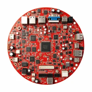
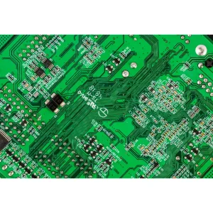
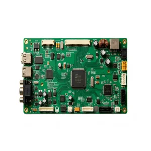
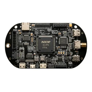
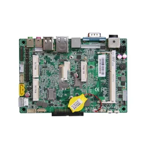

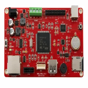
How the Greater Bay Area electronics industrial cluster delivers unrivaled procurement speed, integrated design-for-manufacturability (DFM), and total quality governance.
In modern electronics manufacturing, geographical clustering is not simply a convenience; it represents an exponential velocity advantage. Located in Shenzhen's Bao'an industrial nucleus, our manufacturing facility operates within immediate physical proximity to the world’s most comprehensive component supply chains, specialized bare-board fabrication facilities, automated surface finishing lines, and tooling centers. This allows hardware companies to compress the typical New Product Introduction (NPI) cycle by up to 60% compared to Western and regional competitors.
Access direct distributor lines with Arrow, Avnet, Digi-Key, Mouser, and over 100 verified regional franchised suppliers. Rapid BOM risk mitigation and cross-referencing for hard-to-find silicon or end-of-life (EOL) semiconductors.
Every bare PCB panel, reel of components, and solder paste jar is tagged with unique 2D DataMatrix identifiers. Our closed-loop Manufacturing Execution System (MES) continuously records thermal profiles, pick-and-place nozzle pressures, and optical inspection records.
Eliminate financial risk with frictionless scaling. Hardware teams can build 5 prototype PCBA assemblies for benchtop validation, transition directly into 500-unit pilot runs, and seamlessly scale to 1,000,000 units on high-speed modular SMT lines.
Electronics in medical, automotive, aerospace, and energy domains cannot afford intermittent field failures. Our dedicated cells adhere to rigorous design parameters.
| Industry Sector | Core Compliance Standards | Technical Challenges Addressed | Manufacturing & Validation Controls |
|---|---|---|---|
| Automotive Electronics | IATF 16949:2016 AEC-Q100 / Q200 | Thermal cycling (-40°C to +150°C), sustained vibration, galvanic corrosion resistance, harsh chemical fumes. | Selective automated conformal coating, underfill dispensing, AOI solder fillet height checks, high-temp burn-in chambers. |
| Medical & Life Sciences | ISO 13485:2016 FDA 21 CFR Part 820 | Zero contamination, strict biological insulation, signal-to-noise ratio in low-amplitude physiological sensors. | ESD Class 0 cleanrooms, ionic contamination testing (ROSE test), full device history record (DHR) tracking, 100% functional test logging. |
| Aerospace & Defense | IPC-A-610 Class 3 AS9100D | Outgassing under vacuum, cosmic radiation susceptibility, extreme G-force shock loading, tin whisker mitigation. | Lead-based or precision lead-free alloy selection, robotic staking, 3D computed tomography X-Ray (AXI), serialized microsectioning. |
| High-Power & Renewables | UL 796 / UL 94V-0 IEC 62109 | High creeping distances, high voltage breakdown isolation, massive heat dissipation in GaN/SiC power stages. | Heavy copper (up to 12oz) substrates, direct bonded copper (DBC), dielectric withstand (Hi-Pot) testing up to 5kV, thermal imaging. |
Enterprise procurement managers and VP of Engineering rely on quantifiable criteria to audit offshore electronics manufacturing services.
Before cutting copper or loading reels, our 50+ engineers execute a 130-point Design-for-Manufacturing analysis:
Every volume hardware program executes under strict Advanced Product Quality Planning methodologies:
As microprocessors decrease in silicon node dimensions and edge computing demands unprecedented board real estate density, our factory line technology evolves simultaneously.
Equipped with state-of-the-art multi-head modular mounters capable of placing 01005 passive passives (0.4mm × 0.2mm) and advancing toward 008004 components with a placement accuracy of ±15µm @ 3-sigma.
Traditional optical inspection relies on static thresholding, leading to false alarms and fatigue. Our lines integrate dual-side 3D AOI and multi-slice 3D AXI running neural inference networks to distinguish cosmetic meniscus variations from genuine cold joints.
Supporting complex High-Density Interconnect (HDI) structures up to 10+N+10 configurations, Any-Layer Microvia (ALIVH), ceramic-core substrates, and high-frequency Rogers/PTFE hybrids for 5G mmWave and satellite transmission electronics.
Safeguarding proprietary firmware and schematics while ensuring smooth, tariff-compliant global door-to-door delivery.
Strict Non-Disclosure Agreements (NDAs) precede any technical inquiry. Design files reside on air-gapped, isolated CAD workstations. Firmware flashing occurs via encrypted programmer hardware keys with counter limits, preventing over-flashing.
Full conformance documentation for EU RoHS Directive 2011/65/EU, REACH (EC 1907/2006) SVHC lists, Conflict Minerals Reporting Template (CMRT), and California Proposition 65 with material declarations per BOM line item.
Direct door-to-door delivery with Delivered Duty Paid (DDP) options across 90+ countries including the USA, Germany, the UK, Japan, and Australia. Dedicated bonded storage facilities support split-shipments and Kan-Ban replenishment cycles.
Direct technical answers addressing critical sourcing requirements, quality verification, and line setup capabilities.
Class 2 applies to dedicated service electronics (commercial appliances, modems, consumer hardware) where high reliability is required but uninterrupted service is not critical. Class 3 covers high-reliability electronics (medical implants, airborne radar, automotive powertrain modules) where downtime is intolerable. Class 3 imposes stricter barrel-fill requirements (>75% vs. >50% on through-holes), tighter component misalignment tolerances, stringent BGA voiding thresholds (<15%), and mandatory visual/X-ray verification.
Our supply chain policy mandates purchasing directly from original chip manufacturers (OCM) or authorized franchised distributors. For critical or legacy components sourced from qualified brokers, incoming lots undergo incoming inspection in our certified test laboratory: packaging verification, Barcode/Lot code authenticity, acetone chemical marking wipe tests, decapsulation die microscopy, X-ray lead-frame analysis, and RoHS elemental spectroscopy.
To produce an engineering-validated DFM analysis and firm quote within 24–48 hours, we require: (1) Gerber RS-274X or ODB++ fabrication data, (2) Detailed Bill of Materials (BOM) in Excel with manufacturer name, exact MPN, package designator, and quantity per board, (3) Centroid / Pick-and-Place (XY coordinates) file, and (4) Assembly drawings outlining conformal coating keep-out zones, heat sinks, torque specifications, and functional testing protocols.
Yes. Our experienced engineering team specializes in BOM scrubbing and value engineering. We identify Pin-to-Pin (P2P) functional drop-in replacements, propose minor footprint-compatible silicon alternatives, or adjust passives to enable second-source components without requiring firmware architectural rewrites, dramatically reducing project lead times during global semiconductor allocations.
Beyond SPI, AOI, and X-ray inspection, we design and operate custom Functional Test (FCT) jigs, In-Circuit Test (ICT) bed-of-nails fixtures, boundary-scan JTAG routines, RF wireless calibration (Wi-Fi, BLE, Zigbee, Cellular), high-voltage dielectric isolation (Hi-Pot) testing, and automated burn-in stress cycling to catch early-life semiconductor infant mortality before packaging.
All solder paste lots are logged with cold-storage temperature history, automated warming timers, and centrifugal planetary mixing routines. Reflow ovens are profiled using 9-channel wireless KIC thermal dataloggers mapped to each board’s physical heat mass, ensuring precise liquidus dwell times and peak ramp rates conform strictly to component thermal constraints.
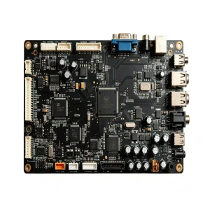
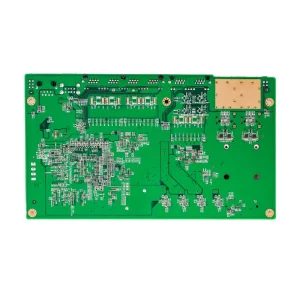
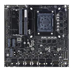
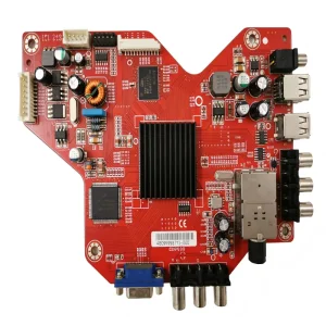
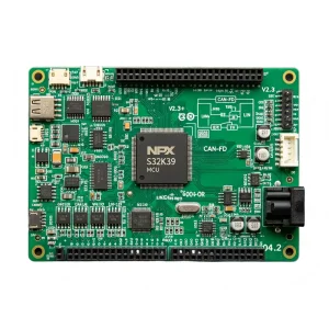
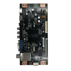
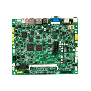
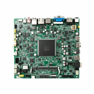
Demonstrating high-density packaging, ruggedized environmental encapsulation, and complex multi-layered power infrastructure.