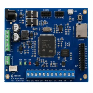

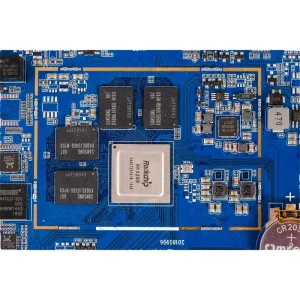
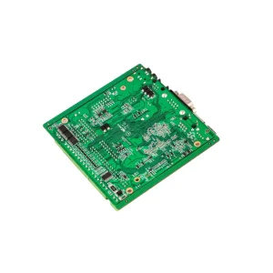
In an era characterized by hyper-dense interconnects, ubiquitous computing, and stringent defect tolerances, electronic manufacturing has transformed from an outsourced assembly commodity into a high-stakes engineering discipline.
The contemporary global electronics ecosystem demands unprecedented integration among electronic hardware architecture, automated component placement, multi-spectral automated optical inspection (AOI), and continuous lifecycle traceability. As original equipment manufacturers (OEMs) navigate market velocity, shortened design revisions, and increasingly volatile semiconductor availability, securing an authentic tier-one EMS Electronic Manufacturing Manufacturer & Factory partner represents the single most decisive variable in ensuring high product reliability, gross margin sustainability, and brand equity protection.
Historically, contract manufacturing relied on the fragmented division of labor: bare printed circuit board (PCB) fabrication was handled by distinct chemical etch facilities, passive and active parts were acquired through spot brokers, surface-mount technology (SMT) assembly was executed on basic pick-and-place lines, and enclosure box-building was relegated to manual downstream stations. Today, modern turnkey EMS manufacturing operates on an entirely unified digital thread. Every bill of materials (BOM) item is mapped dynamically to enterprise resource planning (ERP) systems, component reel barcodes are interfaced with manufacturing execution systems (MES), and placement machines calibrate real-time nozzle pressures against micro-pitch ball grid arrays (BGAs) and quad-flat no-leads (QFN) footprints down to 01005 passives.
This comprehensive whitepaper illuminates the infrastructural pillars governing mission-critical electronic manufacturing services in China's state-of-the-art manufacturing hubs. From engineering design for manufacturability (DFM) verification protocols to advanced thermal profiling, high-frequency signal integrity guarantees, and closed-loop quality audits, this analysis serves as an operational benchmark for engineering executives, hardware system architects, and global procurement directors.
Eliminate inter-vendor friction. STHL centralizes PCB layout review, component supply assurance, SMT/THT assembly, conformal coating, cable assembly, and final testing under one certified management umbrella.
From aerospace cockpit avionics to non-invasive ultrasound imaging arrays, production follows rigorous IPC-A-610 Class 3 workmanship criteria, backed by dual 3D automated X-ray inspection (AXI) validation.
Protected network environments, tamper-evident flash programming benches, and legally binding non-disclosure agreements (NDAs) safeguard OEM proprietary firmware and intellectual schematics before evaluation begins.
Examining the structural, geographical, and technological catalysts that render China's advanced EMS factories the undisputed benchmark for rapid scaling, component procurement depth, and yield predictability.
While basic assembly can theoretically be performed in diverse regions across the globe, high-complexity, high-density electronic assemblies require an interconnected industrial infrastructure that cannot be replicated overnight. Shenzhen's Bao'an and Greater Bay Area manufacturing corridors provide an unmatched operational density where semiconductor suppliers, substrate fabricators, precision toolmakers, packaging specialists, and testing houses coexist within an immediate 30-kilometer radius.
This intense supply chain localization delivers distinct quantitative advantages for global OEMs:
Engineering design modifications, alternate silicon drop-ins, and bespoke multi-layer stack-up prototypes can transition from Gerber CAD release to functional bare board and populated surface-mount assembly within 24 to 48 hours.
STHL maintains strategic sourcing pipelines with over 100 verified component agencies, tier-one franchised distributors (Arrow, Avnet, Digi-Key, Mouser), and original semiconductor fabricators, bypassing unverified spot markets.
In-house quality validation laboratories run XRF spectroscopic elemental composition checks, decapsulation die microscopic imaging, and automated solderability testing to protect high-reliability designs from counterfeit silicon.
Operating a modernized 10,000+ m² facility engineered for zero-defect production runs across prototype, high-mix low-volume, and mass volume regimes.
A deep exploration into precision assembly processes, ultra-miniaturized geometries, intelligent inspection algorithms, and sustainable manufacturing standards.
The relentless demand for edge AI compute, wearable biometric monitoring, and high-frequency RF modules has accelerated the adoption of 0.3mm pitch fine-pitch ball grid arrays (micro-BGAs), wafer-level chip-scale packages (WLCSP), and discrete passive packages down to 01005 (0.4mm × 0.2mm) and 008004. Assembling these components requires micro-aperture electroformed stencils, automated high-precision solder paste inspection (3D SPI) with volume measurement resolutions under 0.1 µm, and high-accuracy pick-and-place systems utilizing multi-camera optical alignment capable of ±15 µm @ 3σ placement accuracy.
Lead-free assemblies governed by RoHS 3 regulations utilize SAC305 (Sn96.5Ag3.0Cu0.5) or specialized low-temperature bismuth alloys requiring precise reflow profiles. The thermal process window between the liquidus temperature (217°C) and the maximum peak component limit (245°C–250°C) is exceptionally narrow. In modern EMS factories, 10-zone to 12-zone forced-convection nitrogen (N2) reflow ovens maintain oxygen concentrations below 500 ppm. This eliminates intermetallic oxidation, minimizes void formation beneath thermal pads and large QFN ground sinks, and guarantees uniform wetting across dissimilar thermal mass areas.
Traditional 2D automated optical inspection cannot adequately evaluate solder fillet wetting, coplanarity, or barrel fill on through-hole pins. Modern EMS operations deploy multi-frequency moiré phase-shift 3D AOI, capable of measuring true component height, coplanarity, and solder meniscus curvature. For hidden joints—such as bottom-terminated components (BTCs), quad flat package under-pads, and multi-tier BGA array spheres—in-line 3D Computed Tomography (AXI) performs non-destructive cross-sectional slicing to measure void ratios against IPC-7095 Class 3 criteria (strictly maintaining voiding below 15%).
Sustainable manufacturing has evolved from a statutory mandate to a core engineering imperative. High-grade EMS facilities deploy closed-loop deionized (DI) water wash systems for ultra-clean ionic residue removal (less than 1.56 µg/NaCl equivalent/cm² per IPC-TM-650). Furthermore, selective robotic conformal coating (using UV-curable, solvent-free acrylics and silicones) shields finished PCBA boards against saline corrosion, chemical contaminants, and dielectric breakdown in humid operational environments.
Aligning certified quality management systems (IATF 16949, ISO 13485, ISO 9001, ISO 14001) with distinct mission profiles and regulatory frameworks.
Automotive subsystems operate under brutal vibrational loads, thermal cycling (-40°C to +125°C), and electrical transients. STHL delivers AEC-Q200 passive qualification, PPAP Level 3 documentation, automated selective wave soldering for heavy power copper buses, and full MES trace logs tied to vehicle identification protocols.
Precision ultrasound probes, laboratory automation, patient telemetry, and life-critical diagnostic monitors necessitate exhaustive device history records (DHR), ISO 14644 Class 8 cleanroom sub-assembly, strict lot-controlled inventory, and complete functional testing simulating real patient physiological loads.
Robust industrial computers, programmable logic controllers (PLCs), high-efficiency boost converters, and motor inverters mandate high-dielectric galvanic isolation, heavy copper traces (up to 4oz+), potting compound encapsulation, and extended burn-in cycles under maximum power ratings to prevent factory floor downtime.
Electronic flight instrument systems (EFIS), wireless mesh gateways, and environmental telemetry stations rely on PTFE/Rogers substrates, controlled differential impedance matching (±5%), aerospace-grade conformal parylene coating, and thermal shock chamber testing running -55°C to +150°C thermal ramps.
Addressing intellectual property protection, dual-sourcing architectures, component obsolescence management, and Total Cost of Ownership (TCO) optimization.
Strict role-based file access controls, internal encrypted data repositories, segregated firmware flashing stations, and enforceable legal confidentiality protocols prevent proprietary technology leaks.
Engineering teams scrub bills of materials against global life-cycle databases, proactively recommending drop-in pin-compatible alternatives before components encounter end-of-life (EOL) or 40+ week allocation spikes.
By identifying layout routing flaws and solder bridging risks via front-end DFM reviews, our engineers eliminate expensive scrap rates, driving down real per-unit cost across production scales.
Direct export clearance pathways, bonded warehouse availability, ESD-certified protective packaging, and established logistics partnerships across 90+ destination countries guarantee zero customs bottlenecks.
In-depth responses resolving critical concerns voiced by hardware architects, sourcing specialists, and quality auditors.
A basic assembly shop merely loads customer-supplied boards and reels onto pick-and-place feeders with minimal oversight. A true Tier-1 EMS provider acts as an integrated extension of your engineering organization. At STHL, this encompasses rigorous pre-manufacturing DFM/DFA engineering audits, direct strategic component procurement across franchised silicon networks, custom ICT/FCT test fixture fabrication, automated nitrogen reflow soldering, selective conformal coating, precision box-build integration, and complete MES serial tracking tying every circuit board to specific solder paste lots and reflow thermal curves.
We enforce strict multi-stage process controls: First, high-precision laser-cut nano-coated stencils ensure clean solder paste release. Second, 3D Solder Paste Inspection (SPI) measures solder deposit volume, area, and height, rejecting uneven deposits before component placement. Third, multi-zone forced convection reflow ovens running pure nitrogen environments reduce surface tension and oxidation. Finally, high-resolution 3D Computed Tomography Automated X-ray Inspection (AXI) confirms void ratios remain under 15%, well within IPC-A-610 Class 3 standards.
To provide an accurate, actionable DFM review and quotation within 24 hours, our engineering team requires: (1) Standard Gerber files (RS-274X format) or ODB++ fabrication archive including drill tables; (2) A complete Bill of Materials (BOM) in Excel format with explicit Manufacturer Part Numbers (MPN), approved alternate parts, reference designators, and package types; (3) Centroid / Pick-and-Place XY coordinate file; and (4) Special testing criteria, firmware binary flashing instructions, or conformal coating mask drawings where applicable.
STHL maintains a dedicated high-mix agile line structure with strictly No Minimum Order Quantity (Zero MOQ). We collaborate with hardware innovators during rapid NPI prototype iterations (from 1 to 50 boards) utilizing the exact same high-precision SMT lines, feeders, and reflow ovens that execute high-volume production orders running into hundreds of thousands of units. This guarantees identical thermal profiles, solder wetting characteristics, and metallurgical reliability when scaling from pilot validation to global mass distribution.
Our quality infrastructure operates under continuous third-party certification audits. Automotive PCBA programs incorporate Failure Mode and Effects Analysis (FMEA), Statistical Process Control (SPC) charting CpK values on solder height, and standard PPAP Level 3 document generation. Medical device builds follow ISO 13485 design traceability, strict ESD-protected cleanroom handling, bio-burden monitoring where required, and tamper-evident Device Master Record (DMR) archiving for a minimum of 10 years.
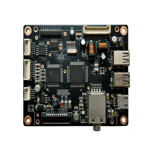

Connect directly with our senior manufacturing engineering team to initiate your comprehensive DFM/DFA analysis, review stack-up impedance calculations, and secure volume BOM cost projections within 24 hours.
Submit Project Gerber & BOM Data