

Explore production-verified PCBA units built with authentic components, zero minimum order constraints, and multi-tier quality inspection from Shenzhen STHL Electronics.
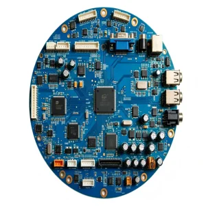


In modern high-mix electronics manufacturing, locating, vetting, and securing high-reliability electronic components demands deep intelligence beyond transactional catalog purchasing.
Semiconductor fabrication distribution is bifurcated across regional clusters. Fabrication plants in North America, Western Europe, and East Asia experience asymmetric supply curves. Lead times for automotive microcontrollers, wide-bandgap MOSFETs, and high-precision op-amps routinely swing from 8 to 52 weeks without algorithmic predictive modeling.
Open-market sourcing presents elevated counterfeit risks—including remarked ICs, recovered dies, and grey-market components. STHL maintains strict tier-1 authorized distributor relationships, supported by AS5553-standard microscopy, solderability verification, and decapsulation analysis before parts enter our cleanrooms.
Product Change Notifications (PCN) and End-of-Life (EOL) obsolescence notices disrupt production lines. Our dedicated engineering desk continuously audits customer bills-of-materials against global obsolescence indexes, proactively identifying pin-compatible Drop-In Replacements (DIR) and Form-Fit-Function (FFF) alternatives before assembly.
A closed-loop electronics manufacturing ecosystem that eliminates supply friction, unifies bare board fabrication with micro-component sourcing, and provides verifiable traceability.
Prior to capital allocation, our engineering team executes automated Design for Manufacturability (DFM) and Design for Assembly (DFA) audits. We verify pad footprint geometries, thermal relief distributions, BGA ball pitches down to 0.35mm, and passives down to 01005 sizing, resolving design flaws before solder paste application.
Leveraging deep component telemetry across 100+ vetted semiconductor agents and manufacturers—including Microchip, STMicroelectronics, TDK, Littelfuse, and Texas Instruments—we identify long-lead bottlenecks and supply secondary approved vendor list (AVL) alternates with zero PCB layout changes.
STHL’s 10,000+ m² Shenzhen facility operates 7 high-speed SMT lines and 2 THT/DIP lines. We manufacture rigid FR-4, flex, rigid-flex, high-Tg, HDI, Rogers, and aluminum substrate boards under one continuous roof, preventing the quality drift and vendor delays caused by fractured manufacturing setups.
How our component sourcing and precision PCBA capabilities translate into reliable end-product performance across regulated global industries.
Compliant with ISO 13485, STHL supplies micro-component assemblies for smart blood glucose monitors, biochemical analyzers, and medical information terminals requiring strict lot traceability, low leakage currents, and conformal encapsulation.
Under IATF 16949 certification, we source AEC-Q100 and AEC-Q200 qualified silicon for in-vehicle communication modules, battery management systems (BMS), and powertrain controllers engineered for continuous thermal cycling.
From industrial wastewater monitors to solar inverters and power quality analyzers, our high-density SMT processes withstand harsh ambient operating conditions, high electromagnetic interference, and dirty field power rails.
We manufacture OEM fly-by-wire (FBW) control units and air data inertial reference units (ADIRU) using ultra-fine pitch placement, 3D automated optical inspection (AOI), and X-ray scrutiny to ensure zero solder joint voiding in avionics computing.
How advances in wide-bandgap semiconductors, optical interconnects, and algorithmic supply networks shape our manufacturing capabilities.
Real-time API integration with Tier-1 component clearinghouses allows sub-second tracking of supply allocation, lead-time drift, and batch authenticity confirmation.
Specialized low-void reflow soldering and heavy-copper substrate thermal routing, maximizing switching frequencies and power densities in compact power topologies.
Precision placement platforms capable of handling ultra-miniaturized dies down to 008004 form factors alongside 0.3mm pitch wafer-level chip scale packages (WLCSP).
Complete traceability pairing raw silicon lot serials with specific pick-and-place nozzle parameters, reflow thermal profiles, and final automated functional testing records.
Clear, engineering-backed answers to the most common questions from hardware developers, sourcing managers, and OEMs.
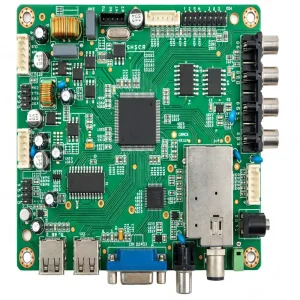
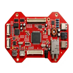
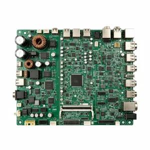
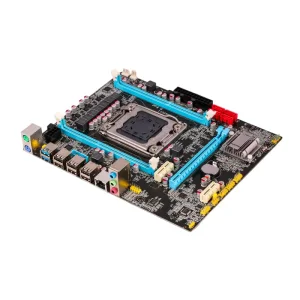
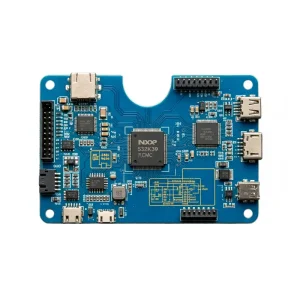
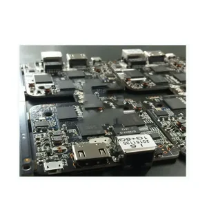
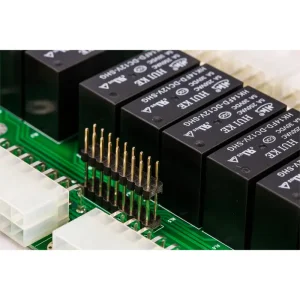
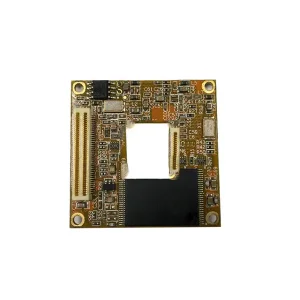
Complete product assemblies engineered with traceable component procurement, multi-stage testing, and turnkey manufacturing support.

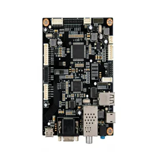
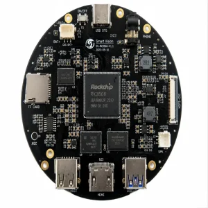
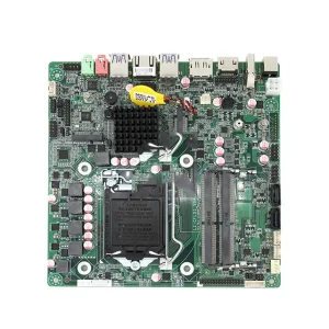
Submit your BOM and Gerber files to our Shenzhen engineering center. Receive a complete DFM report, verified part availability, and competitive factory-direct pricing within 24 hours.