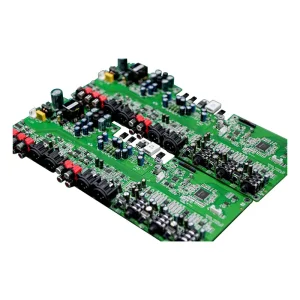
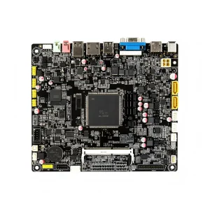
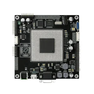
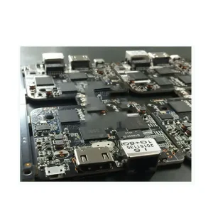
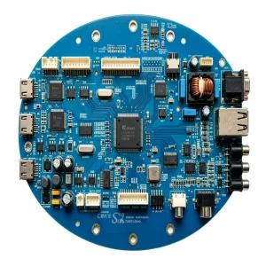
Explore STHL’s specialized turnkey electronics manufacturing applications, engineered under IATF 16949 and ISO 13485 quality standards for extreme environmental resilience.
Addressing high-speed signal attenuation, ultra-fine-pitch BGA escape routing, and thermodynamic stability in sub-0.4mm pitch layouts.
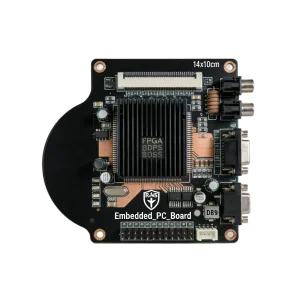
In modern electronic hardware architectures, the physical constraints of traditional through-hole Printed Circuit Boards (PCBs) have created significant bottlenecks for ultra-dense semiconductor integration. As Field Programmable Gate Arrays (FPGAs), System on Chips (SoCs), and AI edge processors transition to ball-grid array (BGA) package pitches below 0.50mm (and down to 0.35mm), conventional mechanical drilling with 0.15mm mechanical bits reaches its physical limit. Mechanical drill wander, aspect-ratio barrel cracking, and large annular ring clearance requirements consume irreplaceable routing channels. High-Density Interconnect (HDI) engineering resolves this fundamental routing impasse through laser-ablated microvias, Sequential Build-Up (SBU) multi-lamination cycles, and Via-In-Pad Plated Over (VIPPO) planarization.
Achieving defect-free microvias requires strict matching between the optical wavelength of the laser system and the absorption characteristics of the dielectric stackup. In modern HDI factories, two laser ablation technologies dominate:
SBU involves building out outer microvia layers symmetrically from a rigid inner core. STHL executes multiple sequential lamination press cycles with precise registration compensation, ensuring registration offsets remain below 25μm across multiple thermal cycles.
Eliminates the mechanical core entirely by electroplating solid copper fill inside microvias across all layers. This allows engineers to freely stack microvias from surface to surface, enabling massive routing density for 5G handhelds and ultra-compact compute modules.
Via-in-Pad Plated Over (IPC-4761 Type VII) requires laser-drilled microvias placed directly within component solder pads, followed by non-conductive/conductive paste filling, copper cap plating, and chemical-mechanical planarization for perfectly flat solder interfaces.
Direct technical comparison between conventional subtractive processing, standard HDI, and ultra-high-density modified Semi-Additive Processes (mSAP).
| Manufacturing Metric | Standard Rigid PCB | Type I / II HDI (1+N+1 / 2+N+2) | Any-Layer HDI (ELIC) | mSAP / Substrate-Like PCB (SLP) |
|---|---|---|---|---|
| Min. Trace Width / Space (L/S) | 100 / 100 μm (4/4 mil) | 65 / 65 μm (2.5/2.5 mil) | 40 / 40 μm (1.6/1.6 mil) | 25 / 25 μm (1.0/1.0 mil) |
| Via Architecture | Mechanical Plated Through-Hole | Staggered Microvias + Core | Stacked Solid Copper Microvias | Direct Laser Microvias + Copper Pillars |
| Min. Finished Hole Diameter | 0.20 mm (8 mil) | 0.10 mm (4 mil) laser microvia | 0.075 mm (3 mil) laser microvia | 0.050 mm (2 mil) ultra-fine microvia |
| Aspect Ratio (Depth:Diameter) | 10:1 (Mechanical Drill) | 0.8:1 to 1:1 (Laser Ablation) | 1:1 (Solid Cu Fill) | 1.2:1 (Pulse Reverse Plating) |
| BGA Escape Pitch Capability | ≥ 0.80 mm pitch | 0.50 mm – 0.65 mm pitch | 0.35 mm – 0.40 mm pitch | < 0.35 mm ultra-fine pitch |
| Dielectric Thickness (Prepreg) | ≥ 100 μm (2116 / 7628 glass) | 50 – 75 μm (1080 / 106 glass) | 35 – 50 μm (1027 / 1017 glass) | 15 – 30 μm (ABF / Unreinforced Film) |
| Layer Count Capability | Up to 64 Layers | Up to 32 Layers | Up to 24 Layers | Up to 16 Layers |
| Surface Finish Options | HASL, ENIG, OSP | ENIG, Immersion Silver, ENEPIG | ENEPIG, Immersion Tin, DIG | Selective Hard Gold + Flash / ENEPIG |
One of the primary causes of latent thermal field failure in stacked HDI microvias is incomplete copper fill, leading to trapped plating chemistry voids. STHL utilizes vertical continuous plating (VCP) lines equipped with periodic pulse-reverse (PPR) rectifiers and advanced organic additive packages (suppressors, accelerators, and levelers). The PPR waveform applies brief cathodic deposition pulses followed by anodic stripping pulses. This preferential electrochemical action suppresses over-plating at the microvia neck while maximizing copper deposition at the bottom of the microvia, yielding a void-free, 100% metallurgical solid copper pillar conforming to IPC-6012 Class 3 requirements.
Mission-critical deployment scenarios where STHL’s HDI engineering, thermal dissipation models, and rigorous qualification protocols drive product success.
Engineered to withstand harsh under-the-hood environments (-40°C to +150°C thermal shock). Built strictly according to IATF 16949 processes for Radar, LiDAR, and Autonomous Driving compute units requiring zero-defect reliability and high copper-wrap barrel integrity.
ISO 13485 certified manufacturing for surgical robotics, ingestible capsules, and patient-worn biometric sensors. Featuring biocompatible surface chemistries, ultra-thin 0.3mm flexible-rigid HDI stackups, and rigorous automated optical inspection (AOI).
Optimized for 112Gbps PAM4 signaling using high-frequency, ultra-low-loss laminates (Megtron 6/7, Rogers 4350B). Precise backdrilling of mechanical core stubs to eliminate signal resonance and jitter, ensuring clean eye diagrams at microwave frequencies.
Designed for severe vibration profiles and rapid pressure fluctuations in airborne control units and smart energy grids. IPC-6012 Class 3 / 3A validation, copper coin thermal integration, and heavy copper inner planes handling high transient surge currents.
How STHL leverages Shenzhen's dense electronic ecosystem, automated robotics, and real-time digital twins to compress NPI schedules and protect BOM integrity.
Shenzhen, China remains the epicenter of the global electronics supply chain, providing unparalleled access to raw substrates, passive component distributors, and precision mechanical fabrication. Operating from our 10,000+ m² smart facility in Bao’an, Shenzhen, STHL transforms this geographic advantage into measurable competitive value for global OEMs. By integrating Industry 4.0 automation across our 7 high-speed SMT lines and dedicated HDI cleanrooms, we eliminate manual human error while slashing lead times from weeks to days.
Eliminates photo-tool film expansion errors. Our digital LDI engines dynamically adjust trace exposure coordinates for real-time laminate dimensional changes across individual panels, maintaining pattern registration within ±12μm.
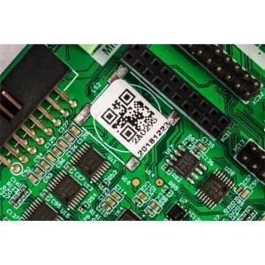
Every single PCB panel is laser-etched with a high-density 2D DataMatrix code. Our Manufacturing Execution System (MES) logs lamination thermal profiles, copper plating current densities, solder paste inspection (SPI) heights, and reflow peak temperatures.
Strategic relationships with original component manufacturers and franchised distributors worldwide ensure immediate stock access. In-house X-ray fluorescence (XRF) material analyzers detect counterfeit components and confirm RoHS lead-free compliance before staging.
Transparent international contract manufacturing engineered to de-risk overseas production for tier-1 OEMs and hardware unicorns.
Client Gerber databases, ODB++ archives, firmware binaries, and proprietary bills of materials (BOMs) reside on air-gapped internal secure servers. Dual-custody role-based access ensures sensitive product blueprints are shielded from third-party exposure.
Our engineering team performs a comprehensive 48-point Design for Manufacturing (DFM) and Assembly (DFA) audit prior to tool commitment. We verify annular ring margins, aspect ratios, component spacing for optical nozzles, and solder mask bridges, preventing costly redesigns.
Our cost engineers recommend form-fit-function alternate passives and active ICs from authorized domestic channels during supply chain pinches, driving down BOM costs by 15%–35% while sustaining strict IPC Class 3 quality thresholds.
From industrial energy management to embedded IoT communications, explore STHL’s finished PCB assembly and box-build capabilities.
Detailed answers to questions raised by hardware designers, layout engineers, and sourcing directors regarding HDI qualification and production.